

Electron emission element, charging device, process cartridge, and image forming apparatus
a technology of electron emission element and charge device, which is applied in the direction of luminescnet screen, discharge tube, instruments, etc., can solve the problems of reducing the life of components, accelerating the deterioration of parts other than photosensitive members, and reducing the resistance of components, so as to achieve the effect of low deterioration of the electron emission material itsel
- Summary
- Abstract
- Description
- Claims
- Application Information
AI Technical Summary
Benefits of technology
Problems solved by technology
Method used
Image

Examples
embodiment 1
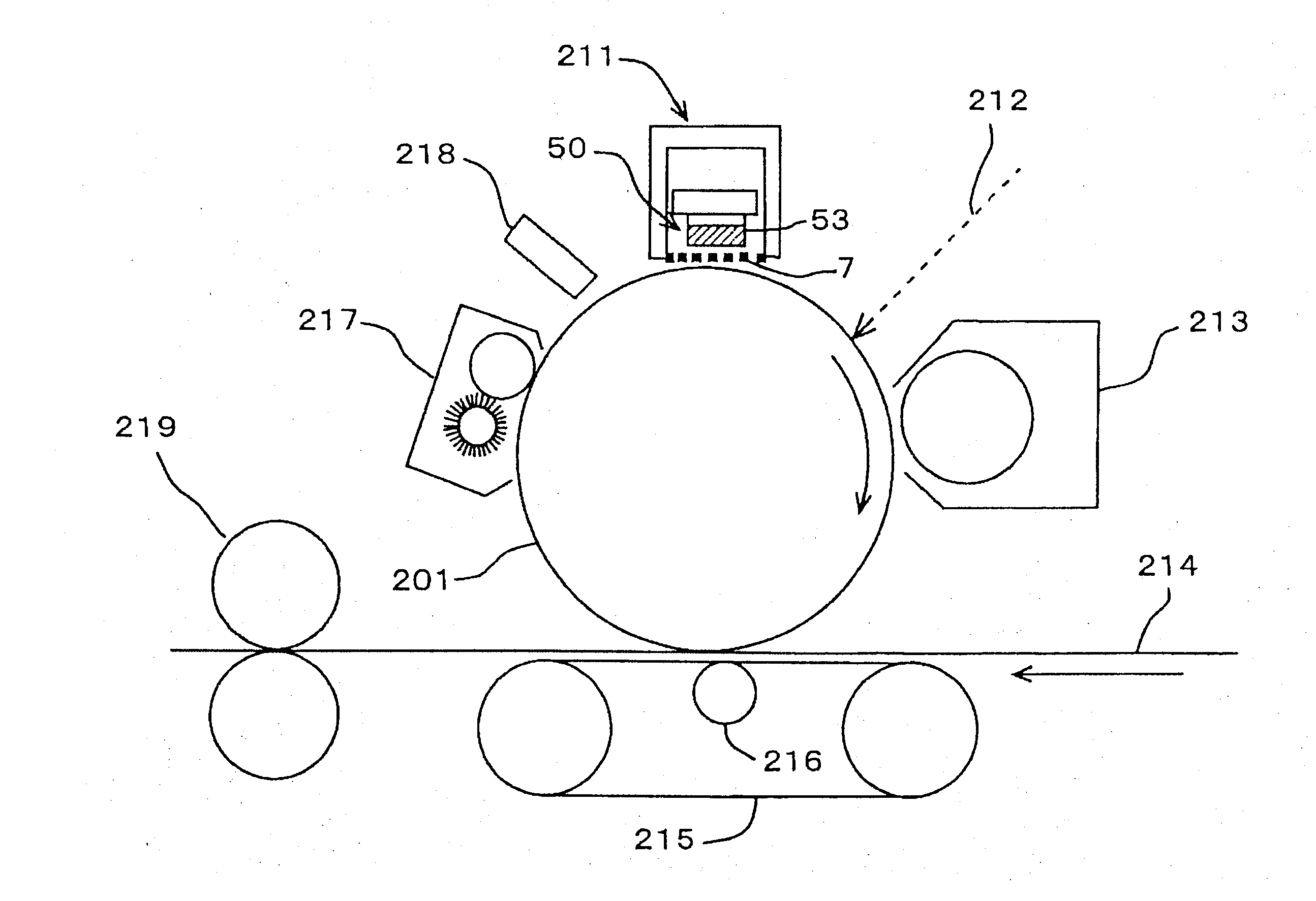
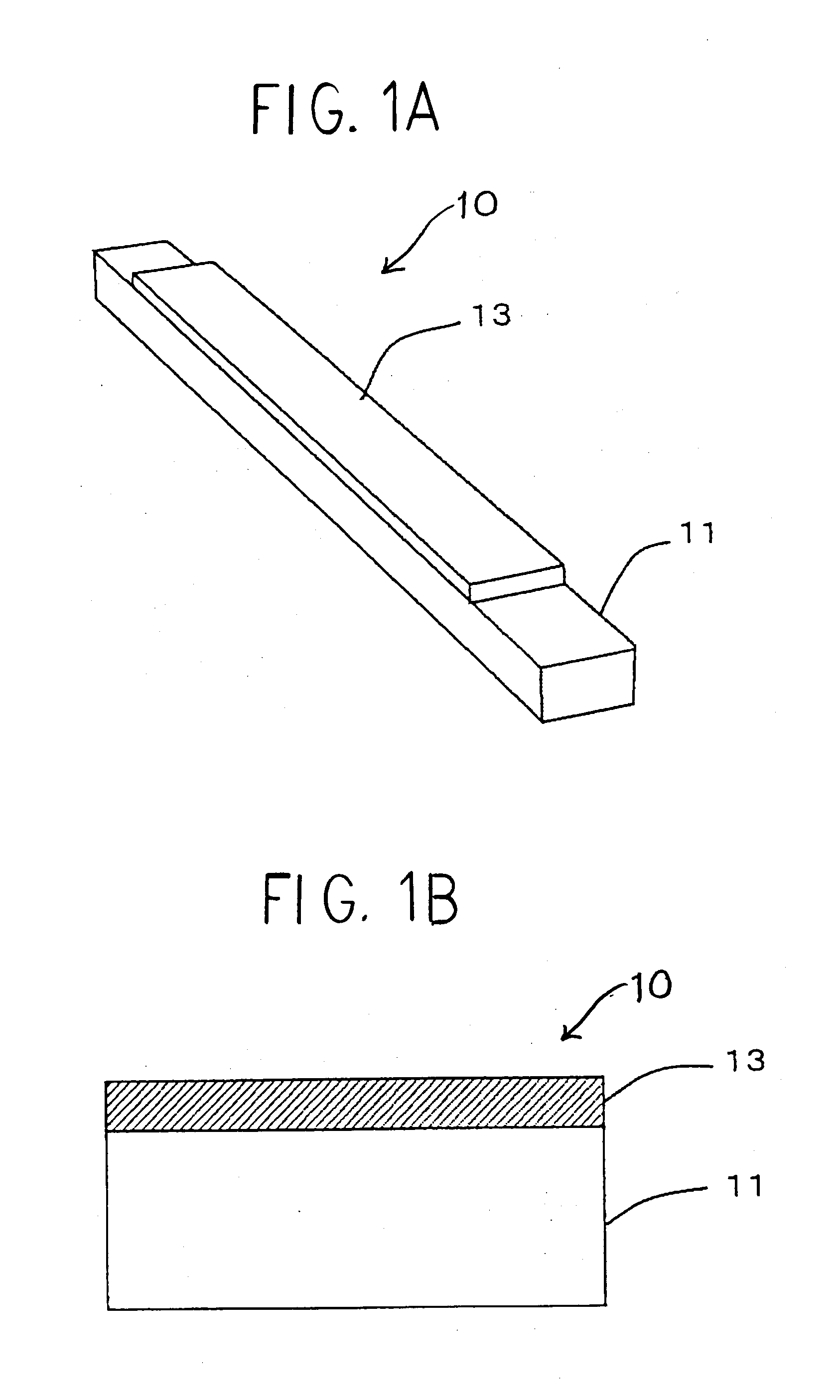
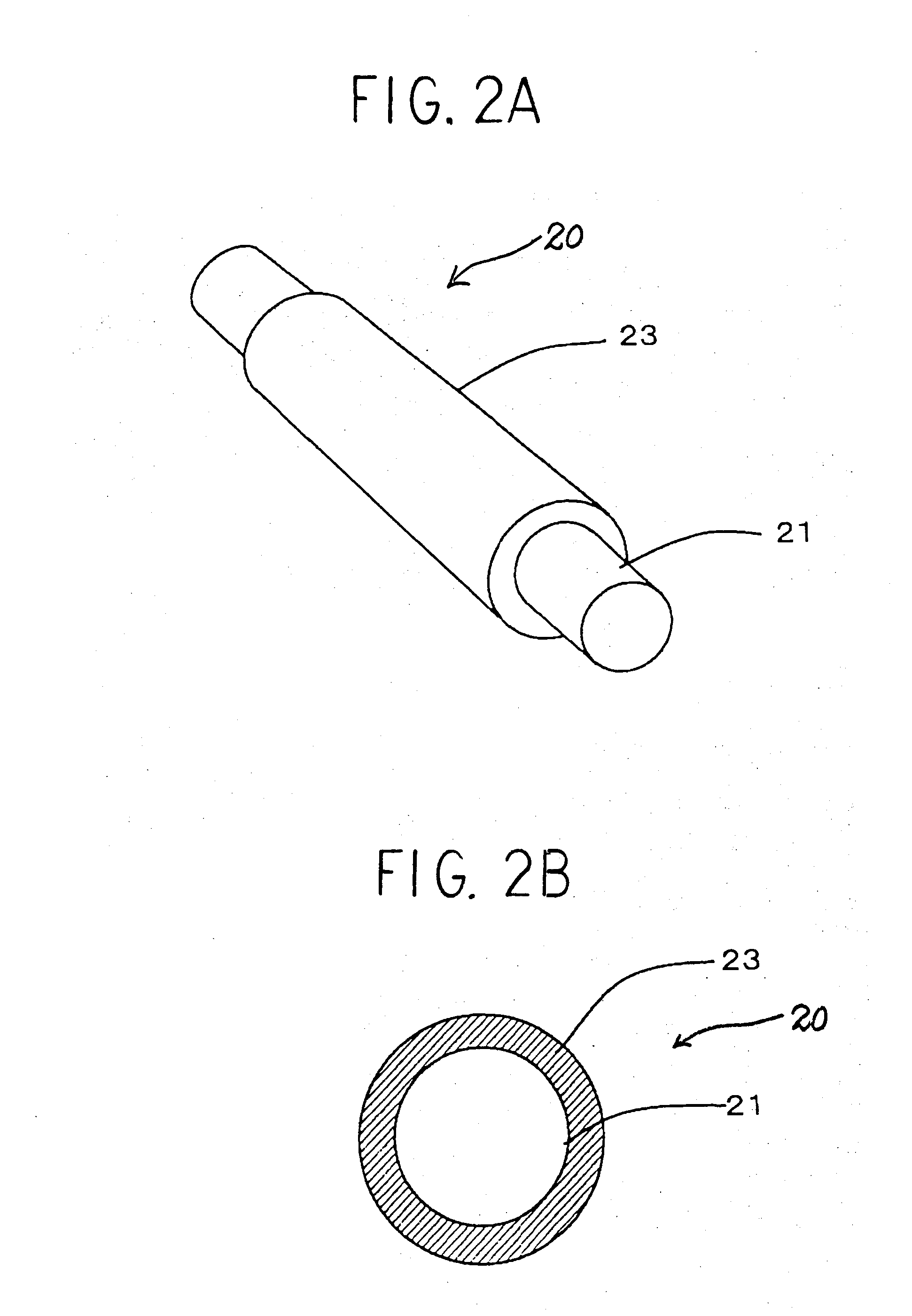
[0084] First, an electron emission element as electron emission means included in the charging device according to the present embodiment is explained with reference to FIGS. 1A, 1B, 2A, and 2B.
[0085]FIGS. 1A and 1B show an example of the structure of an electron emission element. FIG. 1A shows an external view of the electron emission element, and FIG. 1A shows a section through the electron emission element. An electron emission element 10 in FIGS. 1A and 1B is formed from a rectangular rod shaped substrate and metal material 11, on which a boron nitride thin film 13 is fixed.
[0086] Also, FIGS. 2A and 2B show another example of the structure of an electron emission element. FIG. 2A shows an external view of the electron emission element, and FIG. 2B shows a section through the electron emission element. An electron emission element 20 in FIGS. 2A and 2B is formed from a wire shaped substrate and metal material 21, on which a boron nitride powder 23 is dispersed and fixed.
[0087]...
production conditions example 1
[0105] Next, an example of the conditions for producing Sp3-bonded boron nitride is provided.
[0106] Using the reaction vessel 31 shown in FIG. 3, diborane at a flow rate of 10 sccm and ammonia at a flow rate of 20 sccm was introduced into the flow of diluting gas which was a mixture of argon at a flow rate of 2SLM and hydrogen at a flow rate of 50 sccm, introduced from the reaction gas inlet 32. At the same time, the environment was maintained at a pressure of 30 Torr by extracting the gas from the gas outlet 33 using a vacuum pump, which is not shown in the drawings. The environment was maintained at a temperature of 8000° C. by heating, and excimer laser ultra-violet light 36 was radiated towards a silicon substrate 34. After 60 minutes of production time, the target film was obtained. Analysis of the produced thin film by the X-ray diffraction method showed that the material was a hexagonal system crystal, with 5H type polytype structure by Sp3-bonding. The lattice constants wer...
production conditions example 2
[0110] Next, another example of production conditions for Sp3-bonded boron nitride is described.
[0111] Using the reaction vessel 31 shown in FIG. 3, diborane at a flow rate of 10 sccm and ammonia at a flow rate of 20 sccm was introduced into the flow of diluting gas which was a mixture of argon at a flow rate of 2 SLM and hydrogen at a flow rate of 50 sccm, introduced from the reaction gas inlet 32. At the same time, the environment was maintained at a pressure of 30 Torr by extracting the gas from the gas outlet 33 using a vacuum pump, which is not shown in the drawings. An RF plasma 38 of output 800 W and frequency 13.56 MHz was generated from the plasma torch 37. The environment was maintained at a temperature of 900° C. by heating, and excimer laser ultra-violet light 36 was radiated towards a silicon substrate 34. After 60 minutes of production time, the target film was obtained. Analysis of the product was carried out in the same way as production conditions example 1, which ...
PUM
| Property | Measurement | Unit |
|---|---|---|
| thickness | aaaaa | aaaaa |
| thickness | aaaaa | aaaaa |
| thickness | aaaaa | aaaaa |
Abstract
Description
Claims
Application Information