Semiconductor light-emitting device and method for separating semiconductor light-emitting devices

a light-emitting device and semiconductor technology, applied in the direction of solid-state devices, manufacturing tools, welding/soldering/cutting articles, etc., can solve the problems of affecting the absorption efficiency of emitted light, the inability to reduce the operating cost to a certain level or lower, etc., to achieve the effect of reducing the operating cost, and ensuring the low light ab

Inactive Publication Date: 2007-12-27
TOYODA GOSEI CO LTD
View PDF3 Cites 156 Cited by
  • Summary
  • Abstract
  • Description
  • Claims
  • Application Information

AI Technical Summary

Benefits of technology

[0057] Each of the structurally changed portions is provided at the focused portions. Since the structurally changed portion has a leg portion which is formed through filamentation and which extends in the depth direction, the wafer can be reliably split, keeping low light absorption of the device.
[0058] In the internal processing step, the waists (laser-focused portions) are spatially separated from one another along a split line in the wafer such that the waists are arrayed in a dashed-line-like manner. Light-induced embrittled portions are provided at the portions corresponding to the waists in a substrate. Thus, the light-induced embrittled portions are arrayed on the split face and spatially separated from one another along the split line so as to form a dashed-line-like pattern. The light-induced embrittled portions serve as indents in which the substrate material is absent, whereas the portion provided between two light-induced embrittled portions serve as protrusions in which the substrate material is present. According to the separation method of the present invention, each split face (i.e., side wall) of the separated semiconductor light-emitting device chips is provided with indents / protrusions. Therefore, the total light extraction efficiency can be enhanced by the thus-formed side walls (split faces). In addition, since split faces are provided with indents / protrusions during a wafer splitting step, no additional step of enhancing light extraction efficiency is needed, and semiconductor light-emitting devices can be produced at low cost.

Problems solved by technology

However, such methods have drawbacks in that operating cost cannot be reduced to a certain level or lower, due to use of expendable scribers and dicer blades.
In both cases, light extraction efficiency is impaired, since the split face, which is a side surface of the device and which is intrinsically transparent, is no longer transparent, and absorbs a predominant light emitted from the light-emitting device.
However, the width of the melt-affected portion on a split face (a side face of the device) is problematic, and even when a nanosecond pulse laser beam is employed as a pulse laser beam, the melt-affected portion of the separated device has a large area in a side face of the device, resulting in problematic absorption of emitted light.
In this case, if the aforementioned expendable scriber is employed, operating cost cannot be reduced.
Since such light-emitting devices are separated at very small intervals, split faces must be formed so as to be perpendicular to a substrate surface as designed, and slanted split faces are not allowable.
However, the thus-produced chips can only be subjected to the flip-chip bonding process in which the semiconductor-layer-formed surface is affixed on a mounting frame.
Even if the chips are subjected to the face-up chip bonding process in which the surface of the substrate opposite the semiconductor-layer-formed surface is affixed on a frame having a parabolic mirror, external quantum efficiency cannot be enhanced, since a non-light extraction surface of the substrate is coarsened.
In other words, external quantum efficiency of the aforementioned light-emitting diodes depends on the mounting orientation, which is a problem to be solved.
These steps increase an environmental load and, therefore, decrease throughput.
As a result, light-emitting device production cost increases.

Method used


Image

  • Semiconductor light-emitting device and method for separating semiconductor light-emitting devices
  • Semiconductor light-emitting device and method for separating semiconductor light-emitting devices
  • Semiconductor light-emitting device and method for separating semiconductor light-emitting devices

Examples


example 1

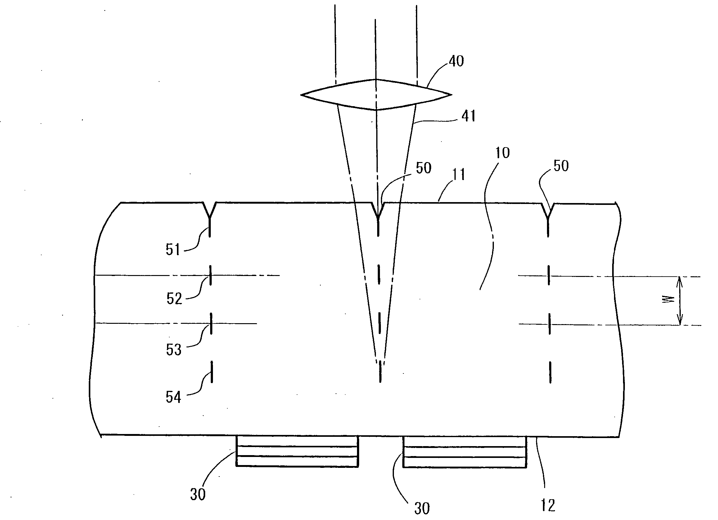
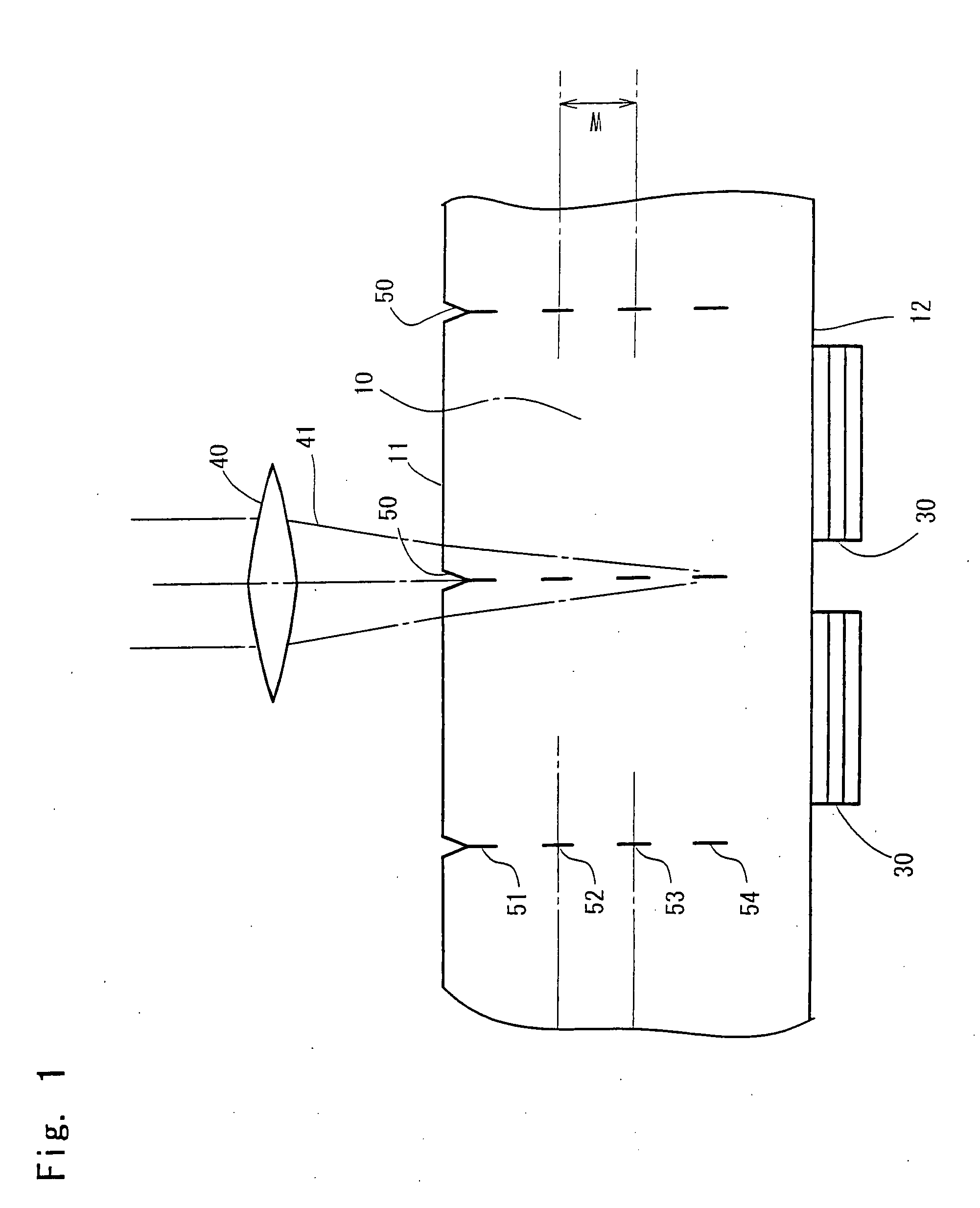
[0091]FIGS. 3A to 3E show the steps included in the method for separating semiconductor light-emitting devices according to one specific example of the present invention. As shown in FIG. 3A, a group III nitride-based compound semiconductor light-emitting device 30 was formed on one surface 12 of the sapphire substrate 10 having a thickness of 140 μm through epitaxial growth, formation of electrodes, and other steps. Subsequently, an unnecessary portion near a split line for separating the group III nitride-based compound semiconductor light-emitting device 30 was removed through etching (FIG. 3B).

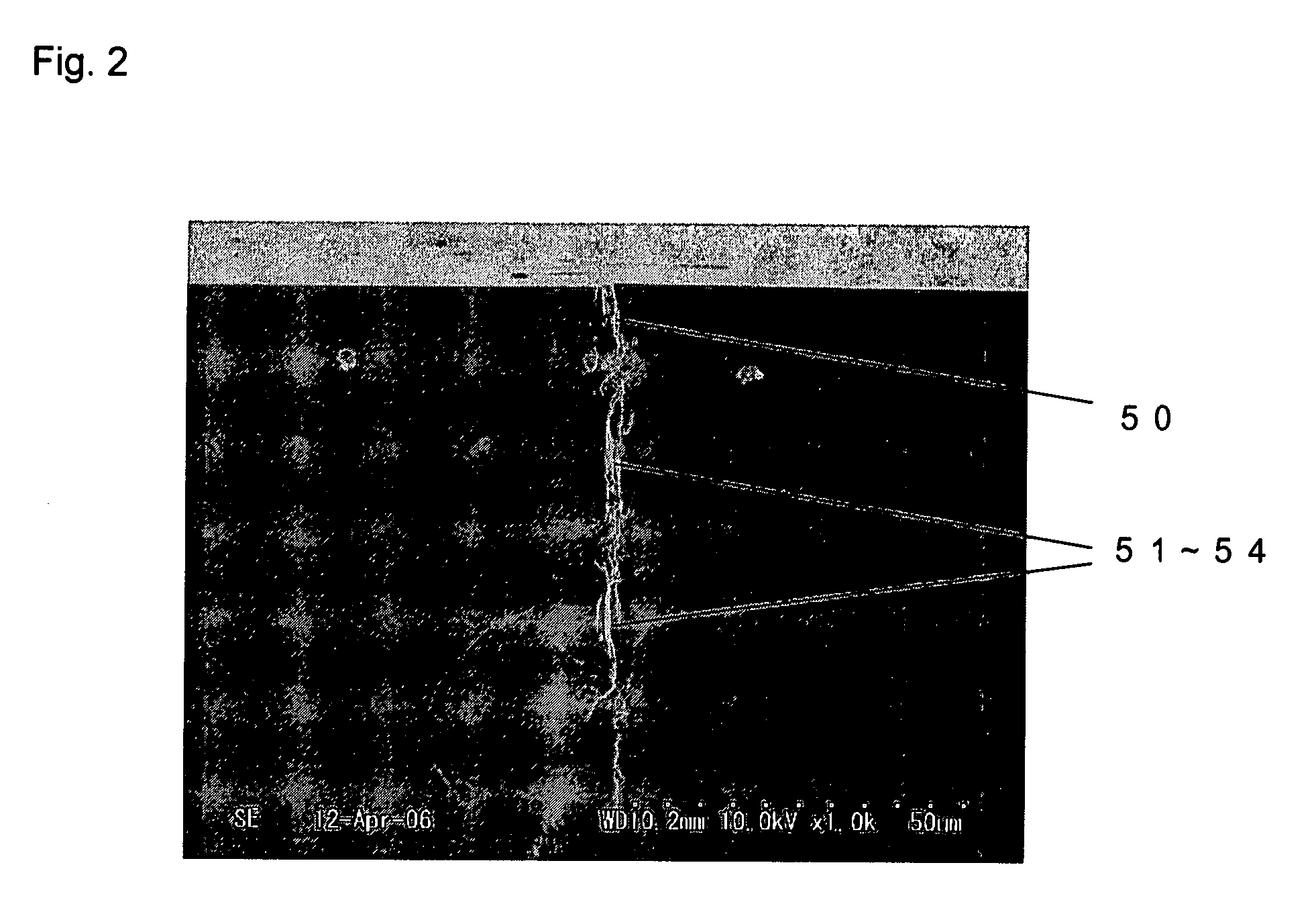
[0092] Next, an adhesive tape 60 was attached to the surface of the sapphire substrate 10 on which the group III nitride-based compound semiconductor light-emitting devices 30 had been formed, and the femtosecond pulse laser beam was scanned on the surface 11, which is a backside of the sapphire substrate 10, whereby the groove 50 and the structurally changed portions 51 to 54 were formed...

example 2

[0143] As shown in FIG. 16, internal embrittling steps 1 to 19 were sequentially performed. Then, steps 20 and 21 were performed so as to form a groove. The process was performed under the following conditions. [0144] Work piece: sapphire single crystal (thickness: t=500 μm) [0145] Laser apparatus: Er, Yb-codoped mode-lock fiber laser base femtosecond laser apparatus [0146] Wavelength: 1.045 μm [0147] Pulse width: 400 fs [0148] Pulse repetition frequency: 100 kHz [0149] Condensing lens: numerical aperture of 0.65, and focal length of 4 mm [0150] Pulse energy after passage of condensing lens: 1.5 μJ [0151] Fluence at beam waist: 160 J / cm2 (calculated) [0152] Power density at beam waist: 400 TW / cm2 (calculated) [0153] Laser beam incident face: c-plane of the sapphire crystal (second surface 111 in FIG. 16) [0154] Laser beam incident direction: normal to C plane (direction indicated by the white arrow in FIG. 16) [0155] Number of internal embrittling steps: 19 rows (rows 1 to 19 in FIG...


PUM

PropertyMeasurementUnit
diameteraaaaaaaaaa
diameteraaaaaaaaaa
thicknessaaaaaaaaaa

Abstract

The invention provides a method for separating semiconductor light-emitting devices formed on a substrate. In the method, a pulse laser beam having a pulse width less than 10 ps in a substrate is focused on the substrate, to thereby cause multi-photon absorption in the substrate. Through multi-photon absorption, a groove is formed through the pulse laser beam along a split line predetermined on a surface of the substrate, the groove being substantially continuous in the direction of the predetermined split line. In addition, internal structurally changed portions are formed through the pulse laser beam at a predetermined depth of the substrate on a predetermined split face, the structurally changed portions being discontinuous in the direction of the predetermined split line. Subsequently, an external force is applied to thereby form a split face along the continuous groove and the discontinuous internal structurally changed portions, whereby the semiconductor light-emitting devices are separated from one another

Description

BACKGROUND OF THE INVENTION [0001] 1. Field of the Invention [0002] The present invention relates to a method for separating semiconductor light-emitting devices formed on a substrate, to thereby yield individual semiconductor light-emitting devices, the method including dividing or splitting a wafer formed of the substrate and the devices provided thereon. The present invention is particularly effective for separating, for example, group III nitride-based compound semiconductor light-emitting devices. As used herein, the term “wafer” collectively refers to substrates which are provided through performing so-called wafer processes (e.g., washing, diffusion ion-implantation, thin film growth, epitaxial growth, photolithography, and formation of electrode) on a transparent substrate. [0003] 2. Background Art [0004] Hitherto, a variety of methods have been proposed for splitting a wafer having group III nitride based compound semiconductor light-emitting devices on a sapphire substrate...

Claims


Application Information

Patent Timeline
Patent Type & Authority Applications(United States)
IPC IPC(8): H01L21/00
CPCB23K26/0057B23K26/0635B23K26/4075B28D5/0011H01L33/0095H01L2224/48091H01L2224/49107H01L2224/73265H01L2224/48247H01L2924/00014B23K26/40B23K26/0624B23K26/53B23K2103/50
Inventor MAEDA, SUSUMUSASAKI, RYUICHIRO
Owner TOYODA GOSEI CO LTD
Why Eureka
Try Eureka