Organic Semiconductor Thin Film, Organic Semiconductor Device, Organic Thin Film Transistor and Organic Electronic Luminescence Element

a technology of organic semiconductors and transistors, applied in the direction of transistors, organic chemistry, thermoelectric devices, etc., can solve the problems of difficult equipment change corresponding to the requirement of large-scale display images, and high equipment and production costs, so as to achieve high carrier mobility

Inactive Publication Date: 2008-02-28
KONICA MINOLTA INC
View PDF3 Cites 20 Cited by
  • Summary
  • Abstract
  • Description
  • Claims
  • Application Information

AI Technical Summary

Benefits of technology

[0066] Using the organic semiconductor thin film according to the present invention, it was possible to provide an organic TFT with a high carrier mobility, a field effect transistor, and in addition, a switching device having said organic TFT or said field effect transistor.

Problems solved by technology

Consequently, the costs for equipment and running the production become very high.
In such the processes for producing the silicon semiconductor, the change of the equipment corresponding to the requirement of large-sizing of the displaying image is difficult because a largely changing in the design of the production apparatus such as the vacuum chamber is necessary.
Further, the material of the substrate is limited to one having a resistivity against heating in the processes since the usual production processes for the TFT using silicon include a process performed at high temperature.
Consequently, glass is only practically usable.
Therefore, the displaying apparatus becomes one which is heavy, lacking in the flexibility and easily broken by falling when the displaying apparatus is constituted by the usual TFT elements.
Such the properties caused by forming the TFT elements on the glass substrate are not suitable for satisfying the requirements for the light mobile thin display accompanied with the progress of the information system.
In such amorphous parts, the overlapping of n-conjugated surface of the thiophene ring is small, and since the carrier movement speed is controlled, satisfactory TFT characteristics have not been obtained.
However, since these polyacene compounds either do not dissolve or are difficult to dissolve in organic solvents, there was the problem that the manufacturing could not be done by coating.
Further, although even thiophene oligomers having no substituent groups, typified by unsubstituted sexythiophene, can easily form π-stacks between molecules and can form a structure with orderly arrangement, they are insoluble like pentacene, and there was the problem that it was not possible to manufacture films except only by evaporation.
In the above manner, it was difficult to obtain a film with high crystallinity and orderly arrangement of molecules while being soluble in an organic solvent.
However, a high temperature is necessary for dissolving in an organic solvent said alkyl substituted pentacene, and also, the solubility was not sufficient.
In addition, although aromatic halogenized hydrocarbons such as trichlorobenzene, etc., have been used to dissolve said alkyl substituted pentacene, but non-halogenic solvents are desirable than these halogen based solvents from the point of view of suitability with the environment, and there were also the problems in manufacturing such as problems in solubility, etc.
However, even in the case of these materials, operations such as heating, etc., are necessary for dissolving in an organic solvent, and sufficient solubility has not been obtained.

Method used


Image

  • Organic Semiconductor Thin Film, Organic Semiconductor Device, Organic Thin Film Transistor and Organic Electronic Luminescence Element
  • Organic Semiconductor Thin Film, Organic Semiconductor Device, Organic Thin Film Transistor and Organic Electronic Luminescence Element
  • Organic Semiconductor Thin Film, Organic Semiconductor Device, Organic Thin Film Transistor and Organic Electronic Luminescence Element

Examples


example 1

[0190]1>>: Present Invention

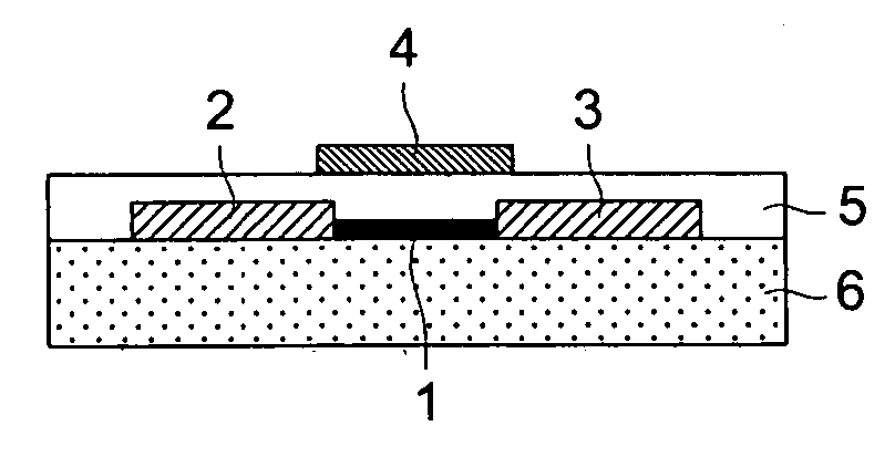
[0191] On a Si wafer with a specific resistivity of 0.02 Ω·cm as the gate electrode, after forming a gate insulation layer by forming a thermal oxide film with a thickness of 200 nm, surface treatment is made using octadecyltrichlorosilane.

[0192] Next, as the organic semiconductor, a cyclohexane solution of the compound (content of 98.6%, Mw / Mn=1) was bubbled with nitrogen gas thereby removing any dissolved oxygen in the solution, the coating was made on the surface of said thermal oxide film (silicon oxide film) using an applicator in a nitrogen gas environment with a pressure of 1.013×10² kPa, and the film was dried at room temperature. At this time, the thickness of the semiconductor layer was 20 nm.

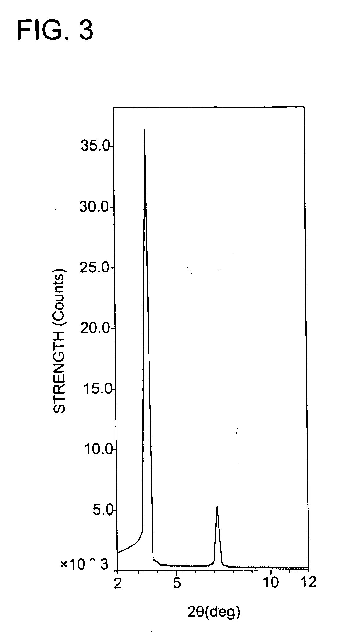
[0193] As a result of evaluating the obtained film by X-ray diffraction, the X-ray diffraction spectrum chart shown in FIG. 3 was obtained. The half width at the diffraction peak with the maximum intensity at 25.1 Å was 0.22°.

[0194] In addition, gold w...

example 2

[0213]>

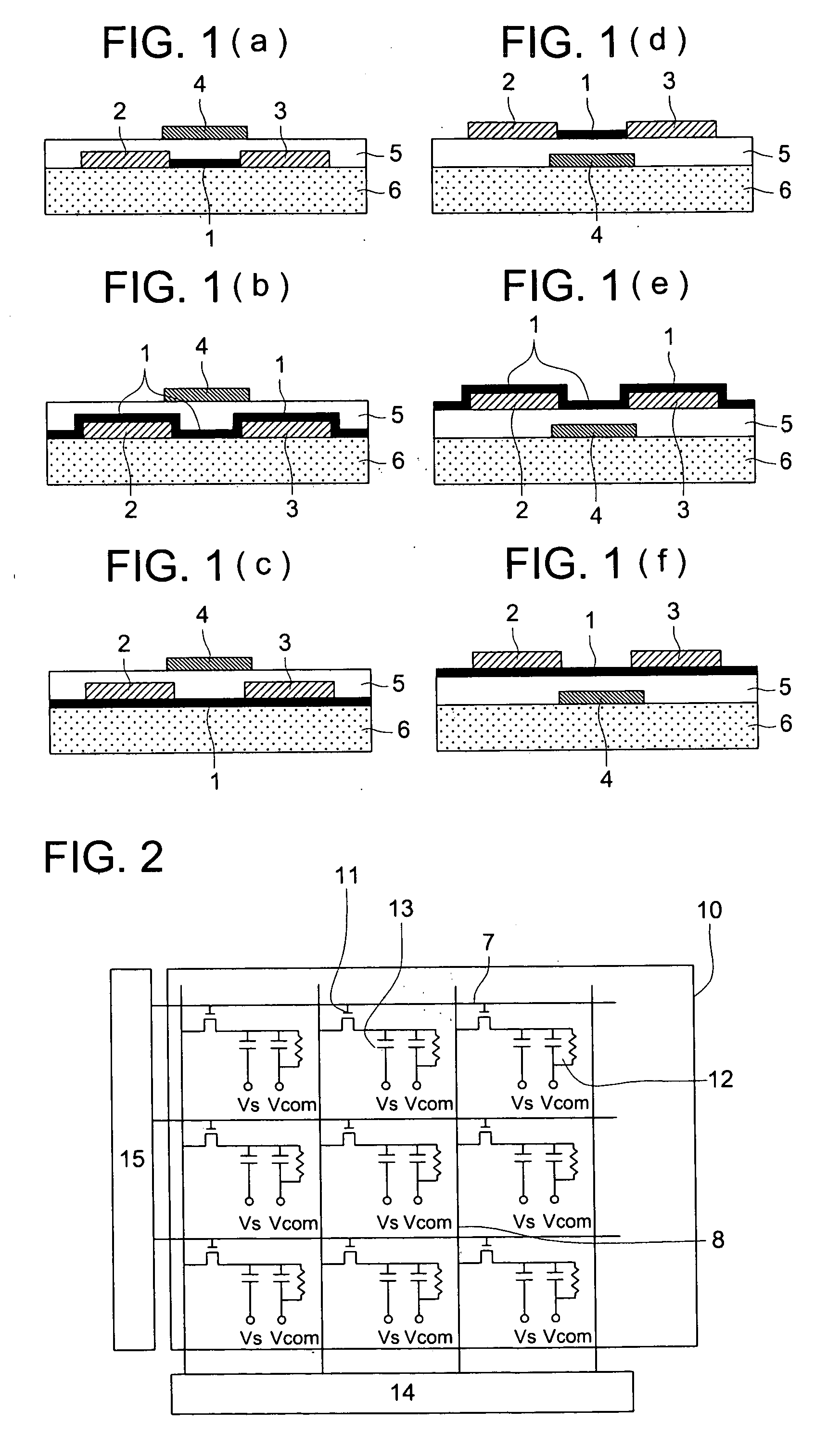
[0214] The method described in Nature, No. 395, pp. 151-154 was referred to for preparing the organic EL device, and a top emission type organic EL device was prepared with a sealed structure as is shown in FIG. 7. Further, in FIG. 7, 101 is the substrate, 102a is the anode, 102b is the organic EL layer (in specific terms, this includes the electron transport layer, the light emitting layer, the hole transport layer), 102c is the cathode, and the light emitting device 102 is formed by the anode 102a, the organic EL layer 102b, and the cathode 102c. Also, the sealed film is indicated by 103. Further, the organic EL device of the present invention can be of the bottom emission type or of the top emission type.

[0215] Although an organic EL and an organic thin film transistor of the present invention were combined (here, the organic thin film transistor of the present invention is used as a switching transistor or as a drive transistor), thereby preparing a light emitting device...


PUM

PropertyMeasurementUnit
temperatureaaaaaaaaaa

Abstract

An organic semiconductor thin film, comprising an organic semiconductor compound, wherein the organic semiconductor thin film is manufactured by a process of forming a film by using a solution or a dispersion at room temperature prepared by mixing the organic semiconductor compound and an organic solvent, and the half width of a diffraction peak having the maximum intensity is 0.4° or less in an X-ray diffraction spectrum of the film.

Description

FIELD OF THE INVENTION [0001] The invention relates to an organic semiconductor thin film, an organic semiconductor device, an organic thin film transistor and an organic electronic luminescence element. BACKGROUND ART [0002] Need of flat panel display for computer rises accompanied with spreading of information terminals. Moreover, electronic paper or digital paper as a thin, light and easily mobile displaying medium is needed because the chance of providing information in a form of electronic signals instead of paper medium is increased accompanied with the progress of information system. [0003] In the planar displaying apparatus, the displaying medium is generally constituted by the use of an element applying liquid crystal, electronic luminescence element (hereafter, referred as organic EL) or electrophoresis. In such the displaying medium, technology in which an active driving element (TFT element) is principally applied for obtaining a uniformity of the brightness and a high r...

Claims


Application Information

Patent Timeline
Patent Type & Authority Applications(United States)
IPC IPC(8): H01L51/30C08F28/06C07D333/10C07D333/18H01L29/786H01L51/00
CPCC07D333/18H01L51/0003H01L51/0545H01L51/0068H01L51/0541H01L51/0036H10K71/12H10K85/113H10K85/655H10K10/466H10K10/464
Inventor TANAKA, TATSUOKITA, HIROSHIHIRAI, KATSURATAKEMURA, CHIYOKOKATAKURA, RIE
Owner KONICA MINOLTA INC
Why Eureka
Try Eureka