

Crystal film, crystal substrate, and semiconductor device
a crystal substrate and semiconductor technology, applied in the field of crystal substrates and crystal substrates, can solve the problems of high-quality crystal film, large process requirements, and inability to achieve crystal growth suitable substrates in nitride iii-v compound semiconductors, and achieve the effect of reducing the dislocation density of the portion formed above the space and reducing the dislocation density of the upper layer on the substra
- Summary
- Abstract
- Description
- Claims
- Application Information
AI Technical Summary
Benefits of technology
Problems solved by technology
Method used
Image

Examples
first embodiment
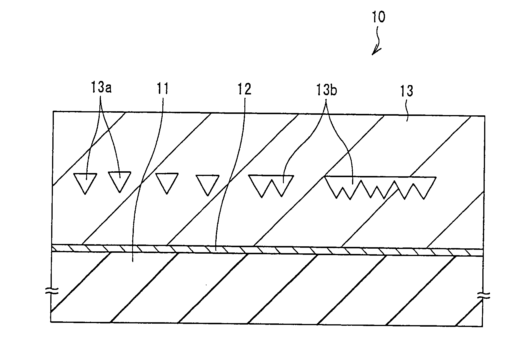
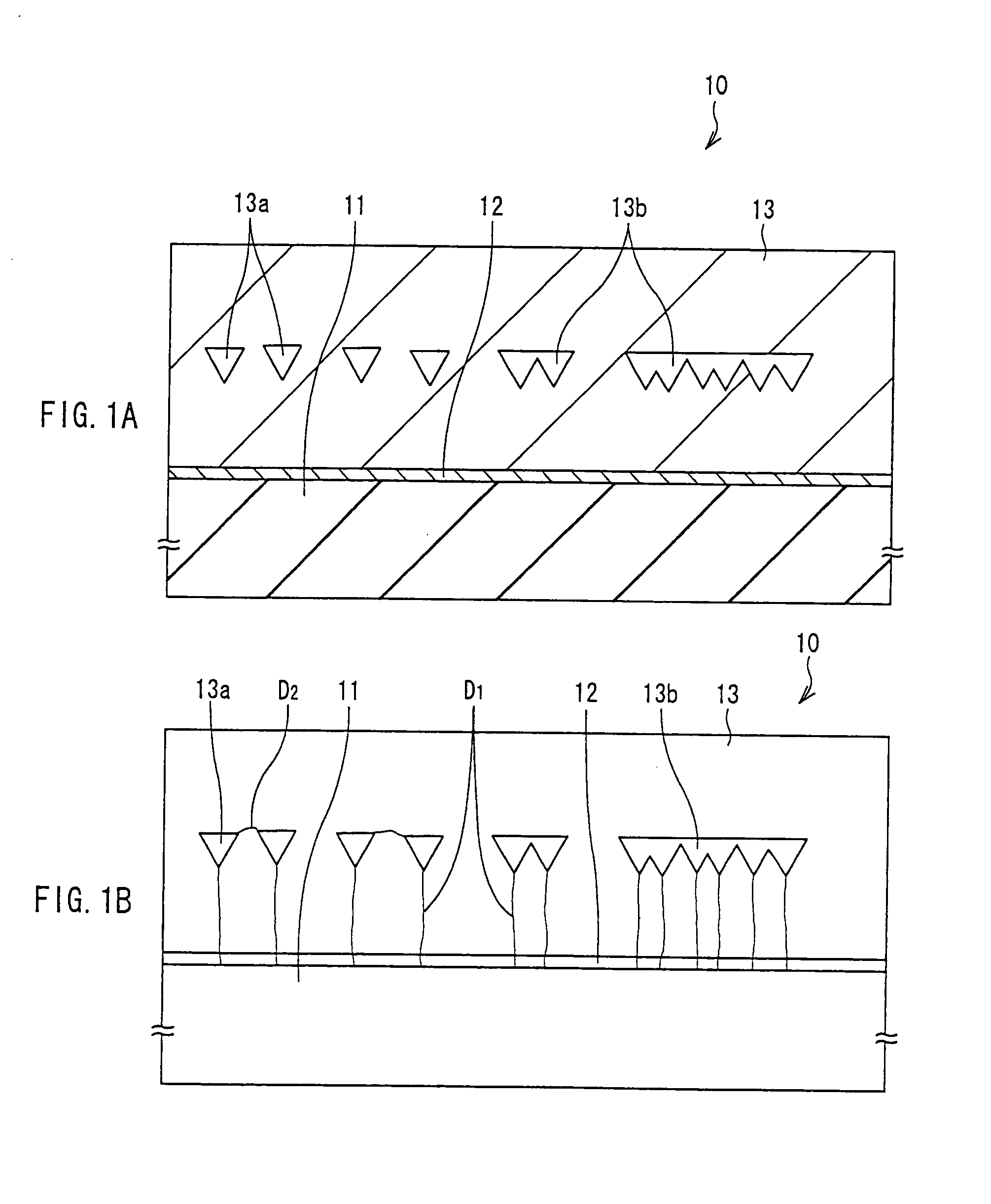
[0035]FIG. 1A shows a sectional structure of a crystal substrate 10 according to a first embodiment of the invention. FIG. 1B is a view showing dislocations of the crystal substrate 10 shown in FIG. 1A. In the crystal substrate 10, a crystal layer 13 is formed on a growth substrate 11 with a buffer layer 12 in between.
[0036] The growth substrate 11 is made of a crystalline material such as sapphire, silicon carbide (SiC), gallium nitride (GaN), gallium arsenide (GaAs), silicon (Si), a composite oxide of magnesium and aluminum (MgAl2O4; spinel), or a composite oxide of lithium and gallium (LiGaO2), and has a thickness of 400 μm, for example. The growth substrate 11 may be made of III-V compounds including at least one element selected from Group 3B elements and at least arsenic (As) and phosphorus (P) selected from Group 5B elements. The crystal substrate having dislocations are widely applicable as the growth substrate 11.
[0037] The buffer layer 12 is a core layer for growing the ...
second embodiment
[0057]FIG. 4A shows a sectional structure of a crystal substrate 20 of a second embodiment. FIG. 4B schematically shows dislocations of the crystal substrate 20 shown in FIG. 4A. The crystal substrate 20 has the same structure as the crystal substrate 10 of the first embodiment except that the crystal substrate 20 comprises a crystal layer 23 instead of the crystal layer 13 of the first embodiment.
[0058] The crystal layer 23 of the embodiment has spaces 23a and 23b like the spaces 13a and 13b of the first embodiment. However, a coat film 21 including, for example at least one of oxygen, nitrogen, fluorine or carbon is provided on the inner surface of the spaces 23a and 23b. The coat film 21 is preferably amorphous to avoid the growth of the crystal thereon. As the material of the coat film 21, a metal material such as aluminum (Al), gallium (Ga), indium (In), magnesium (Mg), zirconium (Zr) or titanium (Ti), silicon (Si) oxide, nitride, fluoride, and carbide are cited. The above met...
third embodiment
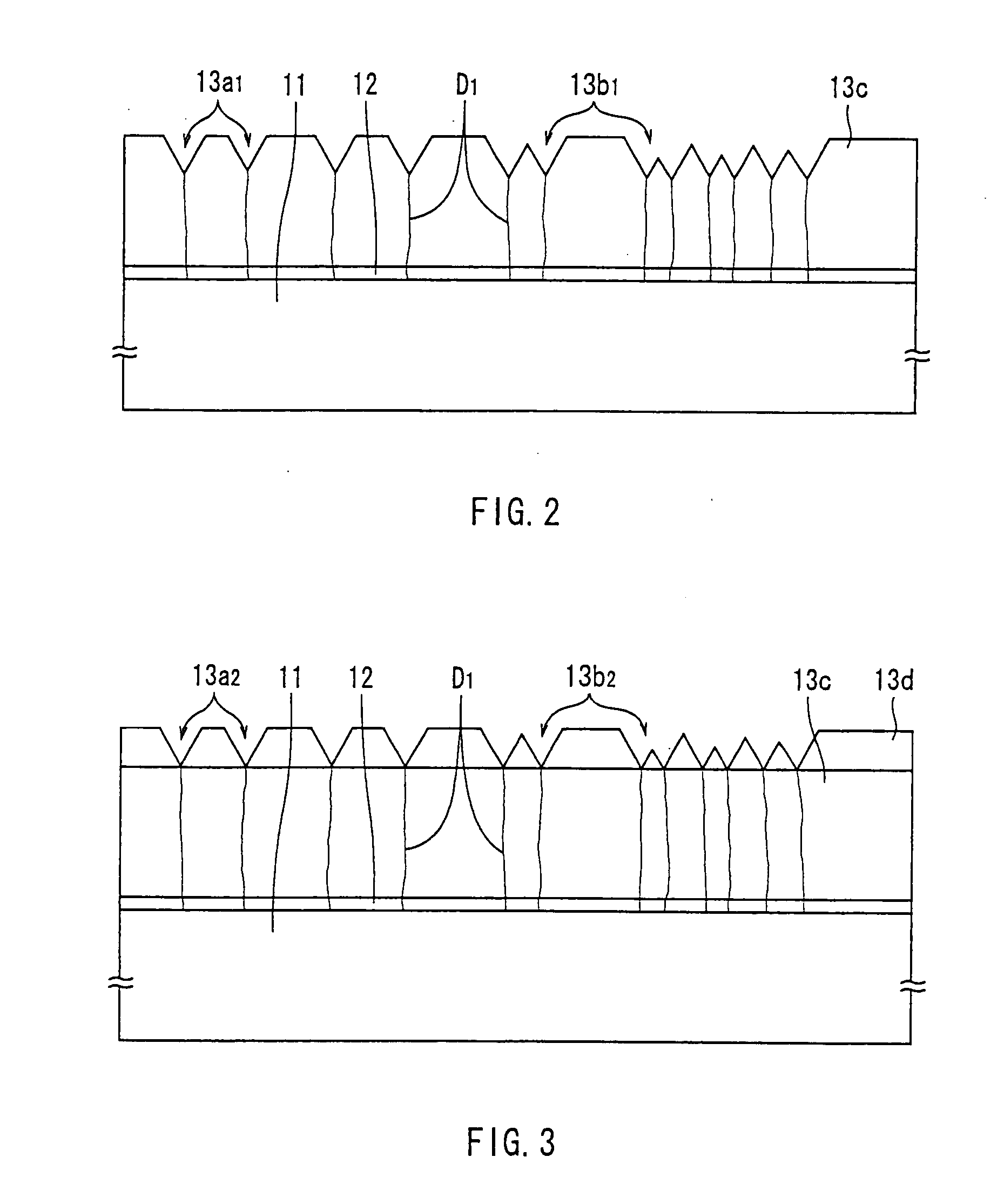
[0064]FIG. 6A shows a sectional structure of a crystal substrate 30 of a third embodiment. FIG. 6B schematically shows the crystal substrate 30 shown in FIG. 6A. The crystal substrate 30 has the same structure as the crystal substrate 10 of the first embodiment except that a crystal layer 33 is provided instead of the crystal layer 13 of the first embodiment. The crystal substrate 30 is fabricated as described hereinbelow.
[0065] First, as shown in FIG. 7, like the first embodiment, etch pits 33a1 and 33b1 are formed on a surface of a lower layer 33c. Subsequently, at least one of oxidation, nitridation, fuluoridation and carbonization is performed on the surface of the lower layer 33c including the etch pits 33a1 and 33b1 to form a surface treatment region 33c1. The surface treatment region 33c1 has a thickness of, for example 1 nm in the thickness direction. Specifically, the surface treatment region 33c1 made of oxide of Group 3B elements is formed by stopping the supply of the s...
PUM
| Property | Measurement | Unit |
|---|---|---|
| temperature | aaaaa | aaaaa |
| thickness | aaaaa | aaaaa |
| thickness | aaaaa | aaaaa |
Abstract
Description
Claims
Application Information