

Processing apparatus with a chamber having therein a high-corrosion-resistant sprayed film
- Summary
- Abstract
- Description
- Claims
- Application Information
AI Technical Summary
Benefits of technology
Problems solved by technology
Method used
Image

Examples
first embodiment
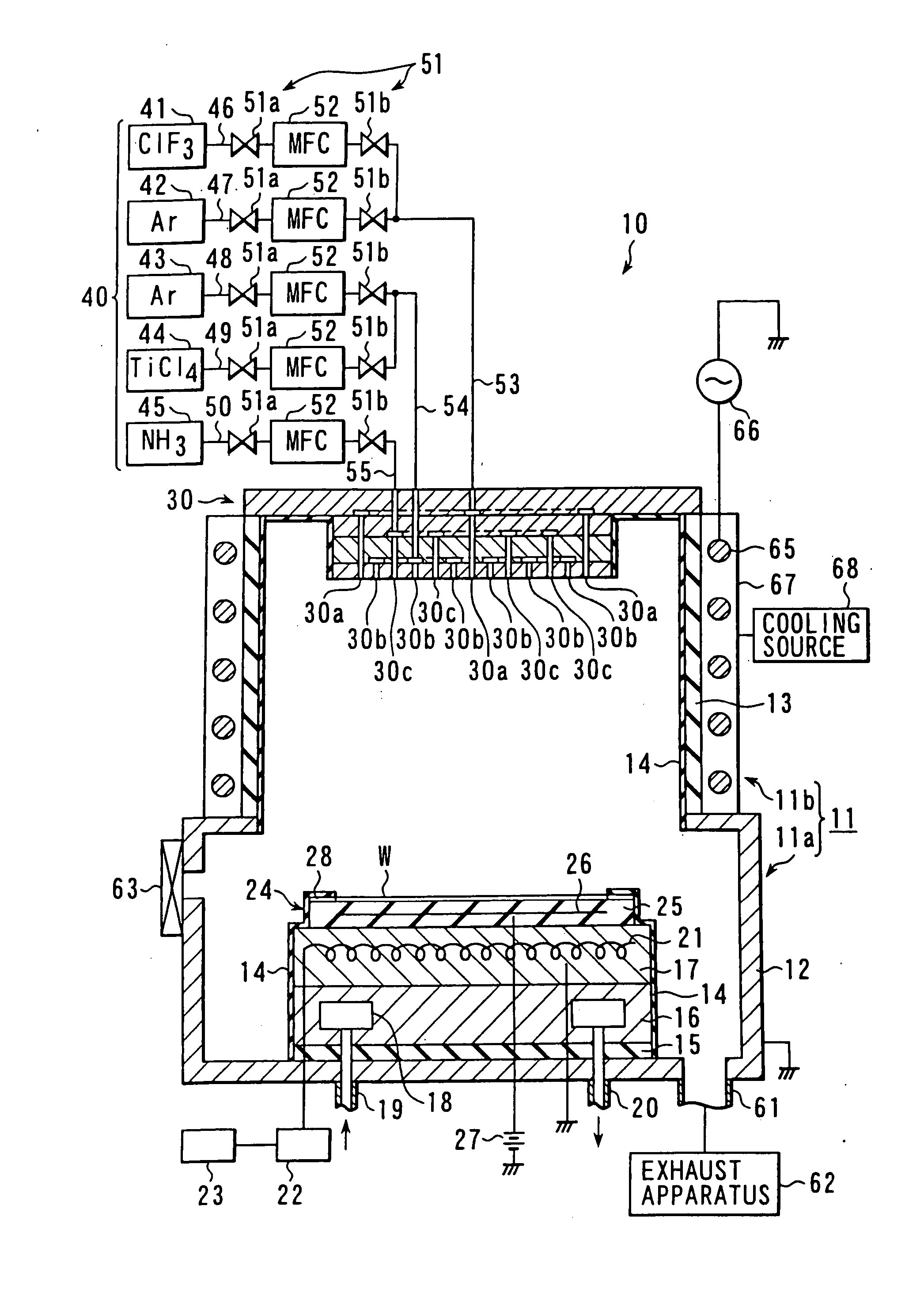
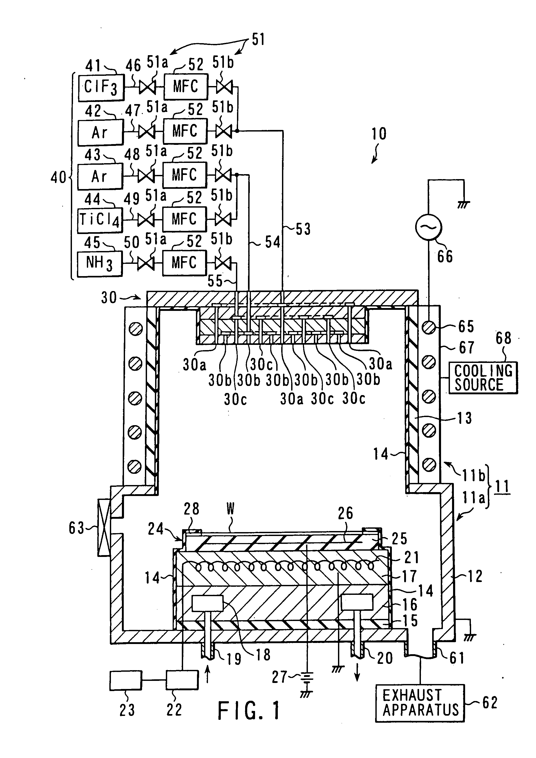
[0042]FIG. 1 is a cross-sectional view showing a practical example applied to a CVD film forming apparatus as the present invention in a processing apparatus having a mounted chamber having a high corrosion-resistant thermal sprayed film.
[0043] The film forming apparatus of the present invention is directed to forming, for example, a TiN thin film. The film forming apparatus 10 includes a chamber 11 having a lower chamber 11a and upper chamber 11 formed as an integral unit in a hermetically sealable way. The upper chamber 11b is made smaller in diameter than the lower chamber 11a. The lower chamber 11a is comprised of an electric conductor 12, such as aluminum, whose surface is anadigation processed for example. The upper chamber 11b comprises a base material 13 of, for example, a ceramic material and a sprayed film 14. The film 14 may contain oxide of Y, Sc, La, Ce, Eu, Dy or the like, or fluoride of one of these metals. The film 14 may be made of a compound of a III-a element of t...
second embodiment
[0068] the present invention will be explained below.
[0069]FIG. 10 is a cross-sectional view showing a CVD apparatus according to the second embodiment. In this embodiment, a chamber, shower head and gas supply system are different in structure from those of the first embodiment. In this Figure, the same reference numerals are employed to designate parts or elements corresponding in structure to those shown in FIG. 1 and any further explanation is, therefore, omitted.
[0070] In this apparatus, an upper chamber 11c is provided above a lower chamber 11a and it is made of a ceramic material, such as Al2O3, SiO2 and AlN. At a shower head member 70 of pipe type provided at the top of the upper chamber 11c, gas discharge holes 70a, 70b and 70c are alternately formed to discharge gases toward a lower zone within the chamber. A gas supply system 40a comprises gas supply sources and valves 51 and mass flow controllers 52 as in the case of the gas supply system 40 as set out above. This embod...
third embodiment
[0080] the present invention will be described below.
[0081]FIG. 11 is a cross-sectional view showing a CVD apparatus according to a third embodiment of the present invention.
[0082] This embodiment constitutes a combined structure of a lower chamber 11a similar to that in the first embodiment shown in FIG. 1 and an upper chamber 11c similar to that of the second embodiment shown in FIG. 10. A sprayed film 14 of mainly Al2O3 and Y2O3 having an insulating property and high corrosion resistance as set out above is formed on the inner wall of the upper chamber 11b. In this embodiment, the same reference numerals are employed to designate parts or elements corresponding in structure to those shown in FIGS. 1 and 10 and any further explanation is, therefore, omitted.
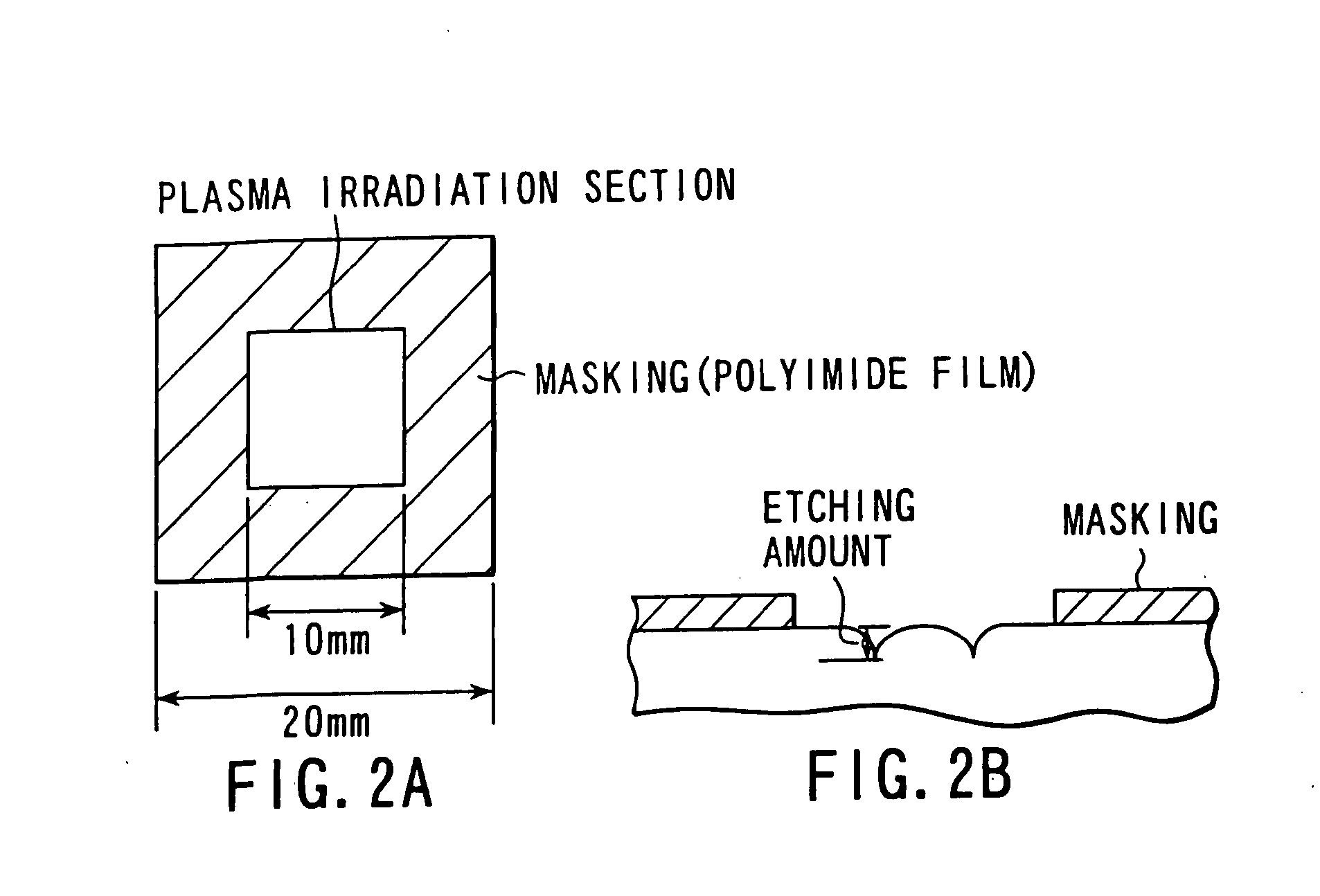
[0083] In the third embodiment, a high-corrosion-resistant sprayed film 14 is formed on the inner wall of the upper chamber 11c and, even if plasma and cleaning gas are contacted with the inner wall, is hard to be etched to p...
PUM
| Property | Measurement | Unit |
|---|---|---|
| Length | aaaaa | aaaaa |
| Weight ratio | aaaaa | aaaaa |
| Electrical resistance | aaaaa | aaaaa |
Abstract
Description
Claims
Application Information