Method for Cleaning Soi Wafer
- Summary
- Abstract
- Description
- Claims
- Application Information
AI Technical Summary
Benefits of technology
Problems solved by technology
Method used
Image

Examples
example 1
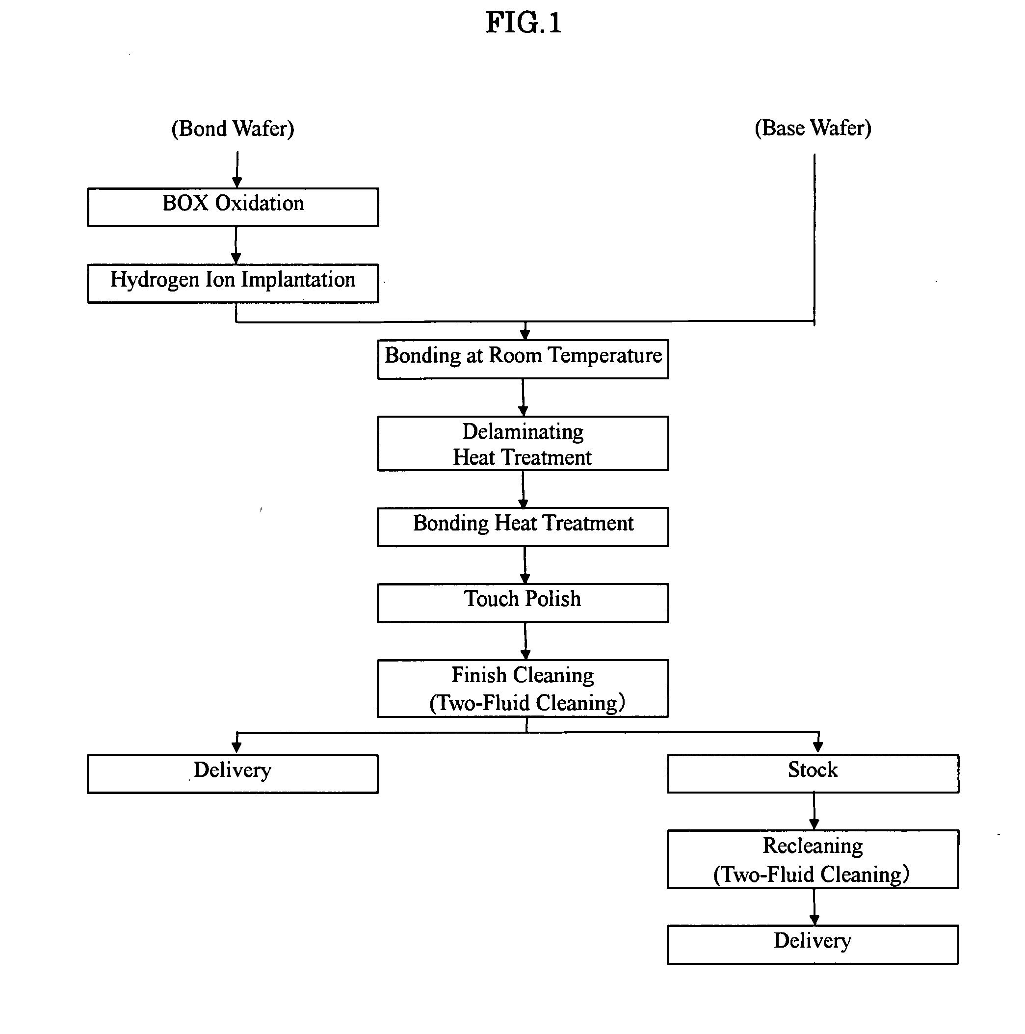
[0056] As a base wafer and a bond wafer, silicon wafers each manufactured by Czochralski method and having a diameter of 300 mm, p-type, (100) orientation, and a resistivity of 10 Ω·cm were prepared.
[0057] On the surface of the bond wafer, an oxide film with a thickness of 1.0 μm was formed. And to the surface of the bond wafer was implanted hydrogen ions to form an enclosed layer.
[0058] Then the ion implanted surface of the bond wafer was brought into contact with the base wafer at room temperature.
[0059] After that, delaminating heat treatment is conducted at 500 degrees C. for 30 minutes in nitrogen gas atmosphere, thereby delaminating and thinning the bond wafer.
[0060] Subsequently, bonding heat treatment was conducted at 1100 degrees C. for 2 hours in an oxidizing atmosphere to bond an SOI layer firmly.
[0061] Next, touch polish was conducted so that its stock removal became about 60 nm to polish the SOI layer.
[0062] Lastly, after rinsing was conducted, two-fluid cleaning ...
example 2
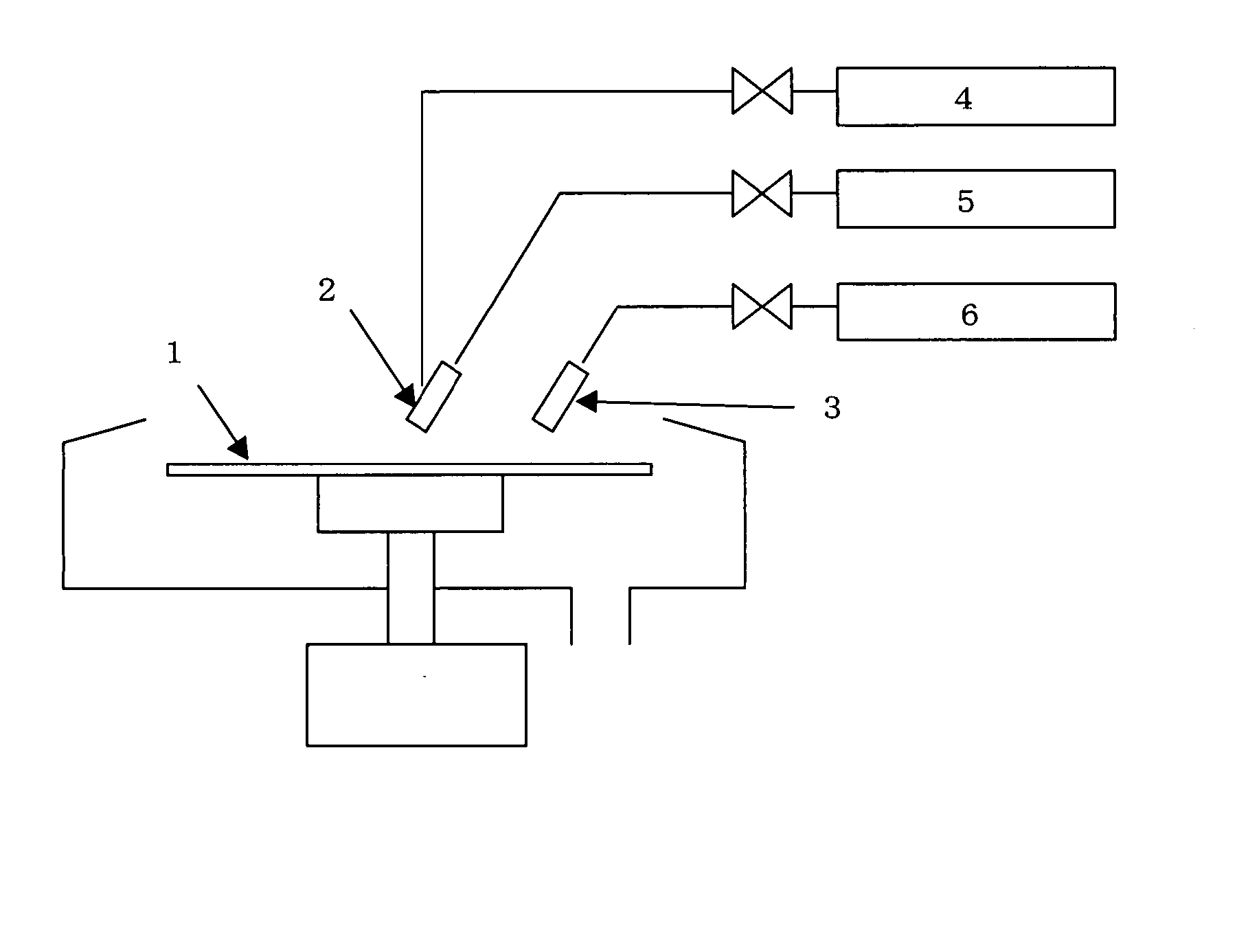
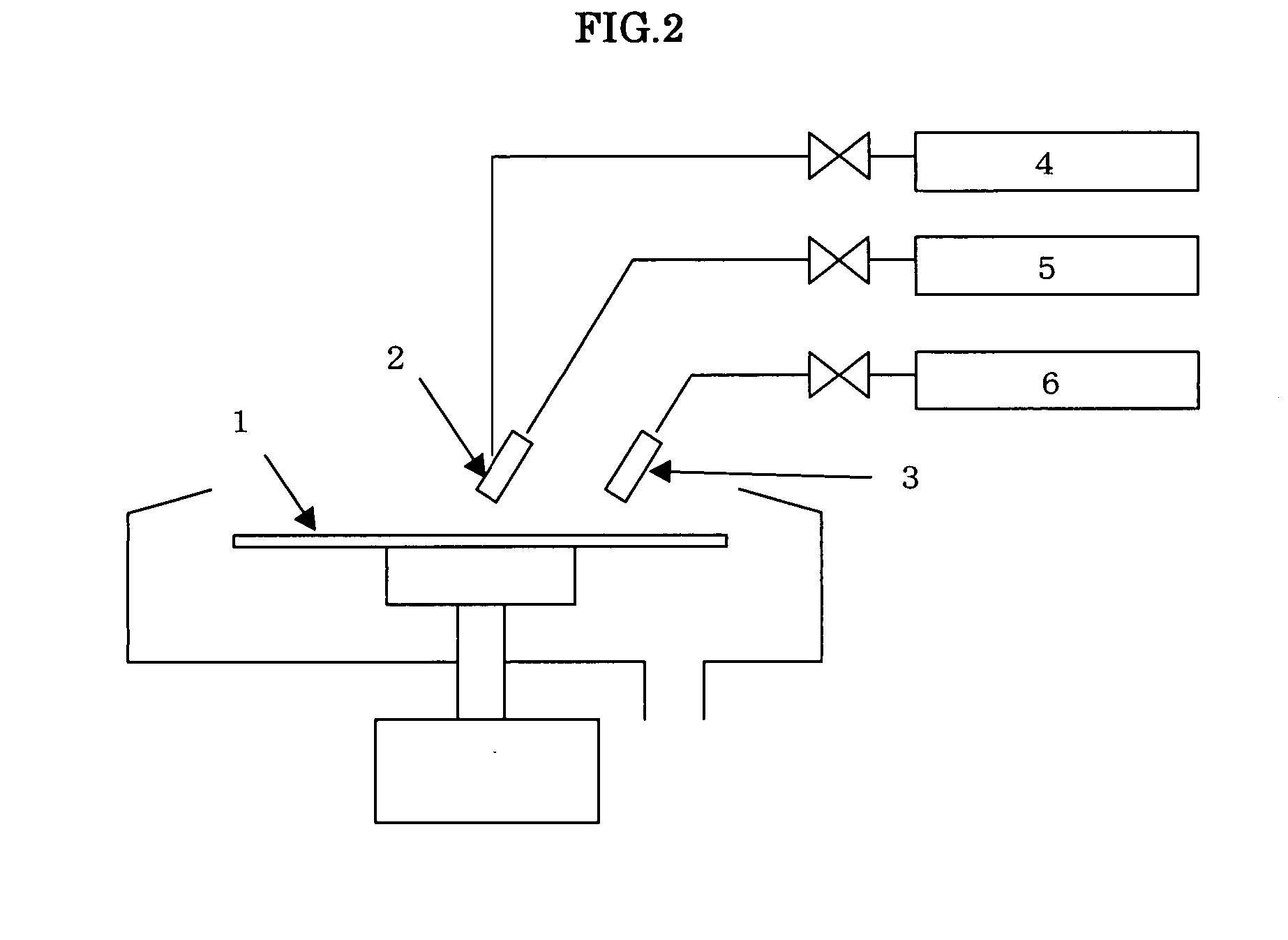
[0064] As with Example 1, silicon wafers were prepared as a base wafer and a bond wafer; the bond wafer was subjected to BOX oxidation, and hydrogen ions were implanted thereto; the bond wafer and the base wafer were brought into contact each other at room temperature, and then subjected to the delaminating heat treatment, the bonding heat treatment, and the touch polish. Lastly, as a finish cleaning, ozone cleaning and two-fluid cleaning were conducted with a cleaning apparatus shown in FIG. 2. In the ozone cleaning, pure water 6 containing ozone of 20 ppm was jetted at a flow rate of 1.2 L / min from a nozzle 3 to a wafer 1 spinning at 60 rpm. At this time, the ozone water 6 had ordinary temperature, a distance between the nozzle 3 and the wafer 1 was 30 mm, the nozzle 3 had an angle of 75°. And the nozzle 3 scanned in the radial direction of the wafer so that it takes 30 seconds per back and forth. Subsequently, the two-fluid cleaning was conducted as with Example 1, and thus manuf...
example 3
[0066] As with Example 2, silicon wafers were prepared as a base wafer and a bond wafer; the bond wafer was subjected to BOX oxidation, and hydrogen ions were implanted thereto; and the bond wafer and the base wafer were brought into contact each other at room temperature, and then subjected to the delaminating heat treatment, the bonding heat treatment, and the touch polish. Lastly, as a finish cleaning, ozone cleaning and two-fluid cleaning were conducted as with Example 2 except that ozone water used in the ozone cleaning had a temperature of 40 degrees C. And thus manufacturing process of the SOI wafer was complete.
[0067] After that, film thickness was measured, and scratches or stains on the surface were inspected. The SOI layer had a film thickness of 30 nm.
PUM
| Property | Measurement | Unit |
|---|---|---|
| Nanoscale particle size | aaaaa | aaaaa |
| Angle | aaaaa | aaaaa |
| Angle | aaaaa | aaaaa |
Abstract
Description
Claims
Application Information
 - Generate Ideas
- Intellectual Property
- Life Sciences
- Materials
- Tech Scout
- Unparalleled Data Quality
- Higher Quality Content
- 60% Fewer Hallucinations
Browse by: Latest US Patents, China's latest patents, Technical Efficacy Thesaurus, Application Domain, Technology Topic, Popular Technical Reports.
© 2025 PatSnap. All rights reserved.Legal|Privacy policy|Modern Slavery Act Transparency Statement|Sitemap|About US| Contact US: help@patsnap.com