Diamond semiconductor element and process for producing the same

a semiconductor element and diamond technology, applied in the field of diamond semiconductor elements, can solve the problems of diamond single crystal having an extremely high density of crystal defects, diamond single crystal having physical derived limitations, and conventional art being incapable of simultaneously satisfying the two requirements, so as to reduce the occurrence of crystal defects and high transconductance of field-effect transistors

Inactive Publication Date: 2008-06-12
NIPPON TELEGRAPH & TELEPHONE CORP
View PDF107 Cites 30 Cited by
  • Summary
  • Abstract
  • Description
  • Claims
  • Application Information

AI Technical Summary

Benefits of technology

001] direction, thereby making it possible to significantly reduce the occurrence of crystal...

Problems solved by technology

However, a diamond single-crystal has the problem of an extremely high density of a crystal defect as compared with that of another semiconductor, for example, silicone, gallium arsenide, indium phosphide, gallium nitride, and the like.
The diamond semiconductor has the physically derived limitation that the channels in which the electron and the hole of a transistor travel are required to be located within 0.1 μm from the surface unlike other semiconductors, for example, silicone, gallium arsenide, indium, gallium nitride, and the like (see non-patent document 3).
This presents fewer problems in the cases of other semiconductors, but in the diamond semiconductor element this is a critical problem resulting from its physical properties that needs to be solved.
In other words, the conventional art is incapable of simultaneously satisfying the two requirements, “a reduction in the source-gate electrode distance and the gate-drain electrode distance” and “an increase in the thickness of the source electrode and the thickness of the drain electrode”.
However, impurities and a large number of crystal defects such as a growth hillock, abnormal growth particles and the like exist in the above diamond single-crystal thin-film.
However, in non-patent document 5, if the temperature is increased for an improvement in crystallinity, when the temperature reaches a certain degree (1200° C.) or more, the conversion to graphite progresses in the diamond thin-film, resulting in an increase in deterioration in crystallinity.
Also, since a p-type semiconductor la...

Method used


Image

  • Diamond semiconductor element and process for producing the same
  • Diamond semiconductor element and process for producing the same
  • Diamond semiconductor element and process for producing the same

Examples


embodiment 1

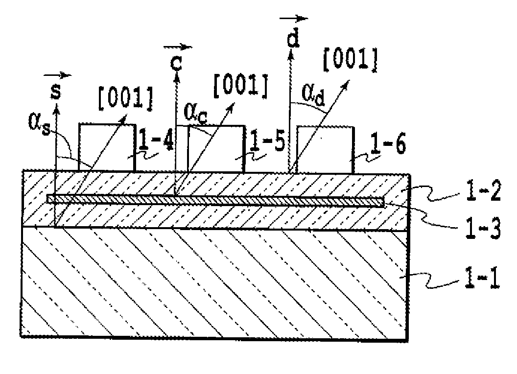
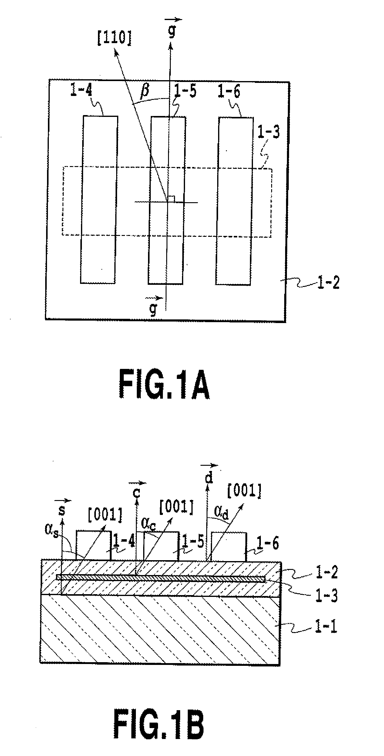
[0248]FIGS. 1A and 1B are schematic diagrams of a diamond semiconductor element according to embodiment 1 of the present invention. As illustrated in the sectional view in FIG. 1B, a single-crystal diamond thin-film 1-2 is formed on a single-crystal diamond substrate 1-1. A two-dimensional hole or electron channel 1-3 is formed in the single-crystal diamond thin-film 1-2. Then, an angle formed by the surface orientation of the single-crystal diamond substrate 1-1 and the crystal axis [001] direction of the single-crystal diamond substrate 1-1 is defined as αs, an angle formed by the surface orientation of the single-crystal diamond thin-film 1-2 and the crystal axis [001] direction of the single-crystal diamond thin-film 1-2 is defined as αd, and an angle formed by the surface orientation of the channel 1-3 and the crystal axis [001] direction of the single-crystal diamond thin-film 1-2 is defined as αc. As illustrated in the top view in FIG. 1A, a source electrode 1-4, a gate elect...

embodiment 2

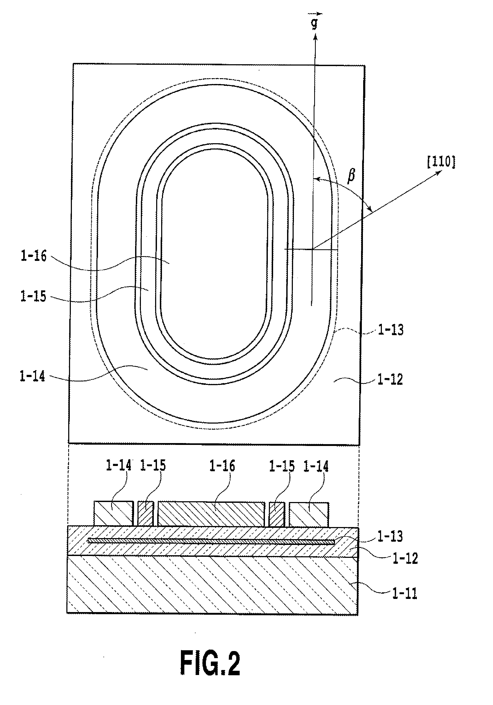
[0267]FIG. 2 is a diagram illustrating the structure of a diamond semiconductor element according to embodiment 2 of the present invention. The structure of embodiment 2 is suitable for high power operation. In embodiment 2, a gate electrode is arranged in the form of a sport ground track. A single-crystal diamond thin-film 1-12 is formed on a single-crystal diamond substrate 1-11 and a two-dimensional hole or electron channel 1-13 is formed inside the single-crystal diamond thin-film. As shown in FIG. 2, the channel has an oval shape. Then, a source electrode 1-14, a gate electrode 1-15 and a drain electrode 1-16 are formed on the surface of the single-crystal diamond thin-film 1-12 above the channel 1-13. The gate electrode 1-15 and the source electrode 1-14 are arranged outward in order so as to encircle the periphery of the oval-shaped drain electrode 1-16 placed innermost.

[0268]FIG. 2 does not clearly show, but in embodiment 2, the surface orientations of the single-crystal dia...

embodiment 3

[0271]FIGS. 7A to 7J illustrate process-steps in producing a diamond semiconductor element according to an embodiment of the present invention. A thin-film 2-1, which is a diamond single-crystal and has a two-dimensional hole channel extending parallel to the surface, (hereinafter referred to as “diamond single-crystal thin-film 2-1”) is prepared (FIG. 07A). Au is evaporated to a thickness of 0.1 μm onto the entire surface of the diamond single-crystal thin-film 2-1 to form an Au thin-film 2-2B (FIG. 7B). Then, the Au thin-film 2-2B is coated with a resist 2-3 with a width of 20 μm in the area in which a gate electrode will be provided (FIG. 7C), and from the above, an Au thin-film 2-2T is evaporated onto the entire surface of the sample (FIG. 7D). At this point, the thickness of the Au thin-film 2-2T is 0.4 μm.

[0272]Next, liftoff is performed on the resist 2-3 to remove the resist 2-3 and part of the Au thin-film 2-2T evaporated onto the resist 2-3 so as to form an aperture 2-7 in ...


PUM

PropertyMeasurementUnit
Fractionaaaaaaaaaa
Fractionaaaaaaaaaa
Fractionaaaaaaaaaa

Abstract

An integrated optical waveguide has a first optical waveguide, a second optical waveguide, and a groove. The second optical waveguide is coupled to the first optical waveguide and has a refractive index that is different from the first optical waveguide. The groove is disposed so as to traverse an optical path of the first optical waveguide and is separated from an interface between the first optical waveguide and the second optical waveguide by a predetermined spacing. The spacing from the interface and the width of the groove are determined such that reflection at a boundary between the first optical waveguide and the second optical waveguide is weakened. A semiconductor board may be disposed at a boundary between the first optical waveguide and the second optical waveguide. In this case, the width of the groove and the thickness of the semiconductor board are determined such that light reflected off an interface between the first optical waveguide and the groove is weakened by light reflected from an interface between the groove and the semiconductor board, and by light reflected from an interface between the semiconductor board and the second optical waveguide.

Description

CROSS-REFERENCE TO RELATED APPLICATIONS[0001]This application is a divisional of U.S. patent application Ser. No. 11 / 577,678, filed Apr. 20, 2007, which is a nationalization of PCT Application No. PCT / JP2006 / 312334, filed Jun. 20, 2006, which claims priority to Japanese Patent Application Nos. 2005-179751 filed Jun. 20, 2005, 2005-270541 filed Sep. 16, 2005, 2005-307231 filed Oct. 21, 2005, and 2006-061838 filed Mar. 7, 2006, which are incorporated herein by reference.FIELD OF THE INVENTION[0002]The present invention relates to a diamond semiconductor element, and more particularly, to a semiconductor element structure in which occurrence of a crystal defect peculiar to a diamond semiconductor element is suppressed, and a process for producing the same.BACKGROUND ART[0003]A diamond has the highest thermal conductivity among a variety of materials, and has the highest breakdown electric field strength among semiconductors. Accordingly, the diamond is the semiconductor material most s...

Claims


Application Information

Patent Timeline
IPC IPC(8): C30B23/00C30B25/00H01L33/00
CPCC23C16/274C23C16/278H01L2924/0002C30B25/105C30B29/04C30B33/02H01L29/045H01L29/1602H01L29/45H01L29/66037H01L29/66045H01L29/66742H01L29/66856H01L29/732H01L29/78H01L29/78684H01L29/812H01L33/0054H01L21/02376H01L21/02433H01L21/02527H01L21/02579H01L21/02609H01L21/0262H01L21/0405H01L21/0415H01L21/324H01L21/02013H01L21/02027H01L2924/00C30B33/06H01L21/18H01L29/73C23C16/27
Inventor KASU, MAKOTOMAKIMOTO, TOSHIKIUEDA, KENJIYAMAUCHI, YOSHIHARU
Owner NIPPON TELEGRAPH & TELEPHONE CORP
Why Eureka
Try Eureka