Semiconductor integrated circuit device

Inactive Publication Date: 2008-07-03
HITACHI LTD
View PDF3 Cites 281 Cited by
  • Summary
  • Abstract
  • Description
  • Claims
  • Application Information

AI Technical Summary

Benefits of technology

[0018]According to the invention, it is possible to attain lower power consumption, larger capacitance, and higher operation speed of a semiconductor integrated circuit device having a DRAM memory. It is particularly useful in a

Problems solved by technology

However, in the case of using an insulation layer having a high permittivity as in hafnium dioxide described above, increase in the leak current due to the deterioration of the insulating performance results in

Method used


Image

  • Semiconductor integrated circuit device
  • Semiconductor integrated circuit device
  • Semiconductor integrated circuit device

Examples


embodiment 1

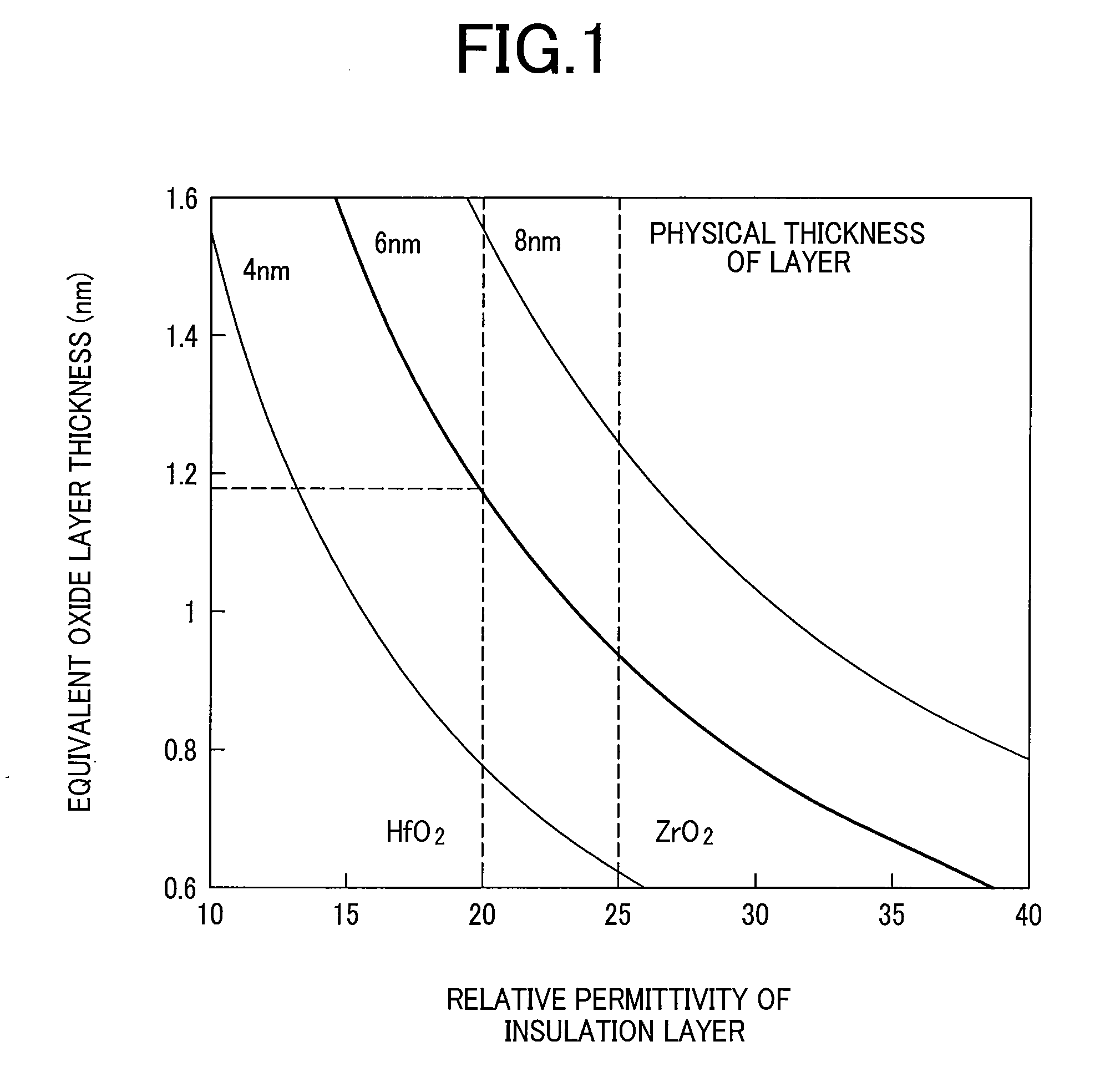
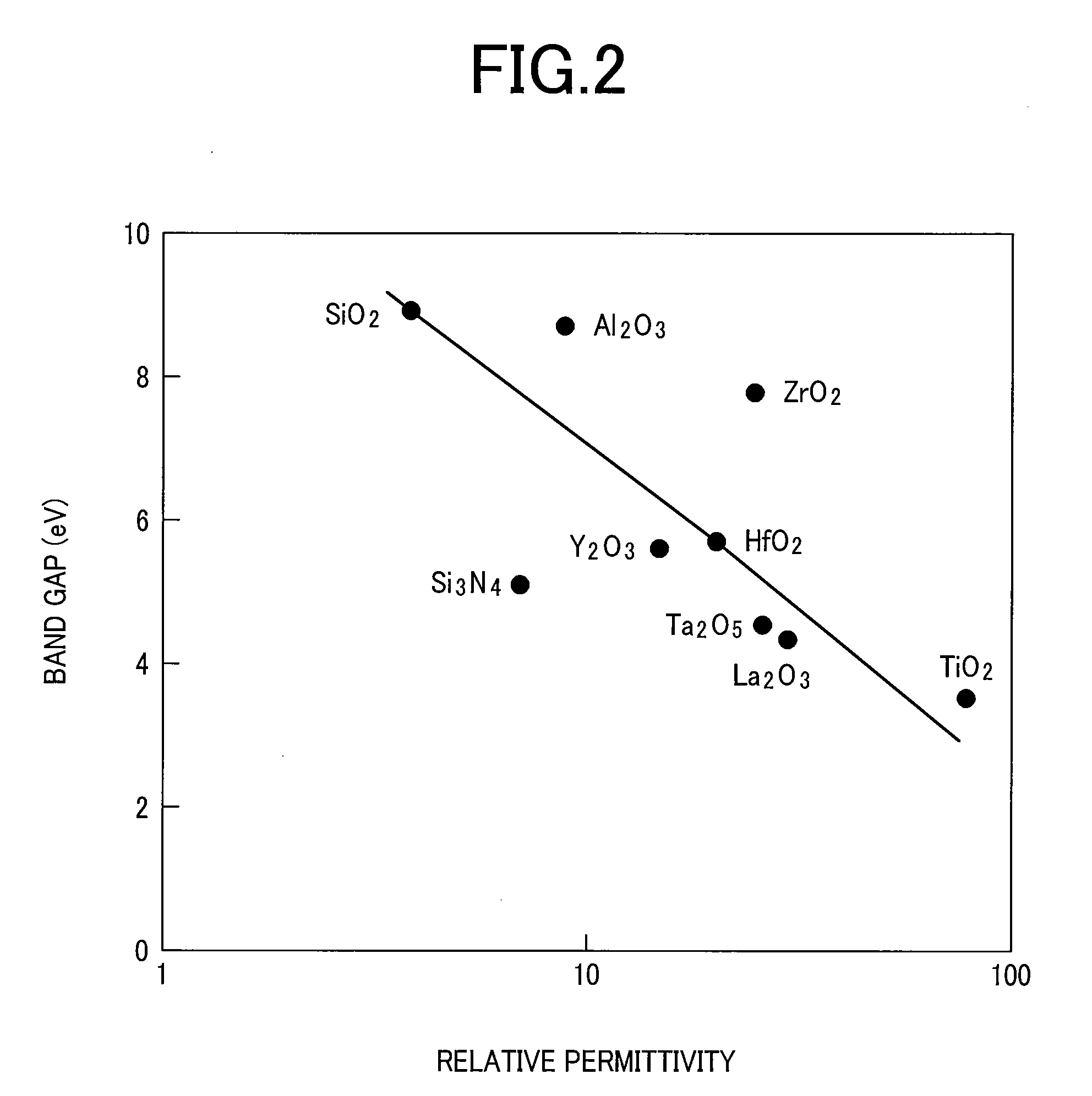
[0072]As described above, in the capacitor of the invention, a first electrode (upper electrode) uses one of members of ruthenium and ruthenium oxide and a second electrode (lower electrode) uses at least one element selected from the group consisting of titanium nitride, titanium, tantalum nitride, tantalum, tungsten nitride, tungsten, phosphorus-doped polysilicon, gold, silver, cupper, and platinum. Further, on the premise for the selection of the first and the second electrode materials, a capacitor insulation layer and a corresponding cap insulation layer were studied. Since the group of materials for the second electrode are those known so far, detailed descriptions therefor are to be omitted. The thickness for each of the members is as described below. The first electrode (upper electrode) is selected within a range from 5 nm to 30 nm, the second electrode (lower electrode) is selected within a range from 5 nm to 30 nm, and the capacitor insulation layer is selected within a r...

embodiment 2

[0116]It is considered that the result shown in Embodiment 1 may be obtained also in the case of reversing the relation of the capacitor up side down. That is, ruthenium is used for the lower electrode and hafnium dioxide is used as the insulation layer. Since ruthenium diffuses into hafnium dioxide when stacking ruthenium and hafnium dioxide, tantalum pentoxide is inserted as the cap insulation layer to the boundary. Finally, titanium nitride is formed as the upper electrode. Since also the capacitor of this structure results in a problem shown in Embodiment 1 that ruthenium diffuses into hafnium dioxide to increase scattering of the leak current density, the cap insulation layer of tantalum pentoxide is inserted to the boundary to solve the problem and the reaction can be suppressed.

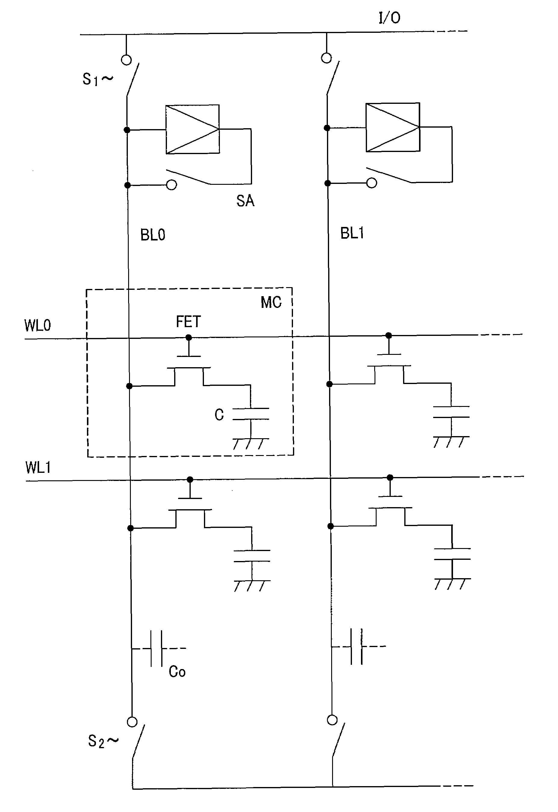
[0117]A method of manufacturing a DRAM memory capacitor having a capacitor suitable to a second embodiment is to be described. Also in this example, since the invention concerns a structure of a memory...


PUM


Abstract

A DRAM capacitor uses ruthenium or ruthenium oxide as an upper electrode and hafnium dioxide or zirconium oxide as an insulation layer. The DRAM capacitor is intended to suppress diffusion of ruthenium, etc. into hafnium dioxide. Tantalum pentoxide or niobium oxide having a higher permittivity than that of the insulation layer is inserted as a cap insulation layer to the boundary between the upper electrode of ruthenium or ruthenium oxide and the insulation layer of hafnium dioxide or zirconium oxide to thereby suppress diffusion of ruthenium, etc. into hafnium dioxide, etc.

Description

CLAIM OF PRIORITY[0001]The present application claims priority from Japanese application JP 2006-351721 filed on Dec. 27, 2006, the content of which is hereby incorporated by reference into this application.BACKGROUND OF THE INVENTION[0002]1. Field of the Invention[0003]The present invention relates to a constitution of a capacitor of a DRAM (Dynamic Random Access Memory) which is a memory for storing information by accumulating charges in the capacitor.[0004]2. Description of the Related Art[0005]Refinement of semiconductor devices has proceeded with an aim of improving the performance. In the memory cell of DRAM, while the occupied area thereto has been decreased along with refinement, a capacitor formed in the memory cell is required to have a constant capacitance irrespective of generations in order to prevent reading failure. Accordingly, increase in the density of the capacitance is demanded for the development of capacitors in the next generation. To make the density of the c...

Claims


Application Information

Patent Timeline
IPC IPC(8): H01L29/94
CPCH01L28/65H01L27/10852H10B12/033H10B12/00
Inventor TONOMURA, OSAMUMIKI, HIROSHISEKIGUCHI, TOMOKOTAKEDA, KENICHI
Owner HITACHI LTD
Why Eureka
Try Eureka