Novel, semiconductor-based, large-area, flexible, electronic devices

a technology of electronic devices and semiconductors, applied in the direction of final product manufacturing, natural mineral layered products, water-setting substance layered products, etc., can solve the problems of unrealized solar energy promise, prohibitive cost of single crystal substrates, unfavorable price/performance metric, etc., and achieve good lattice matching

Inactive Publication Date: 2008-09-11
GOYAL AMIT
View PDF10 Cites 97 Cited by
  • Summary
  • Abstract
  • Description
  • Claims
  • Application Information

AI Technical Summary

Benefits of technology

[0097]The semiconductor template layer can be a “graded semiconductor template” layer with multiple laye

Problems solved by technology

However, for the past two decades, the promise of solar energy has remained unrealized.
This is primarily because of the unfavorable price/performance metric of solar cells being manufactured today.
While a complete understanding of the microstructural features which limit the performance are still unclear, it is reasonably well established that recombination at grain boundaries, intragrain defects and impurities is critical.
Most thin-film solar cells are based on polycrystalline device layers since the cost of single crystal substrates is prohibitively expensive.
Because they are polycrystalline, they do no

Method used


Image

  • Novel, semiconductor-based, large-area, flexible, electronic devices
  • Novel, semiconductor-based, large-area, flexible, electronic devices
  • Novel, semiconductor-based, large-area, flexible, electronic devices

Examples


example 1

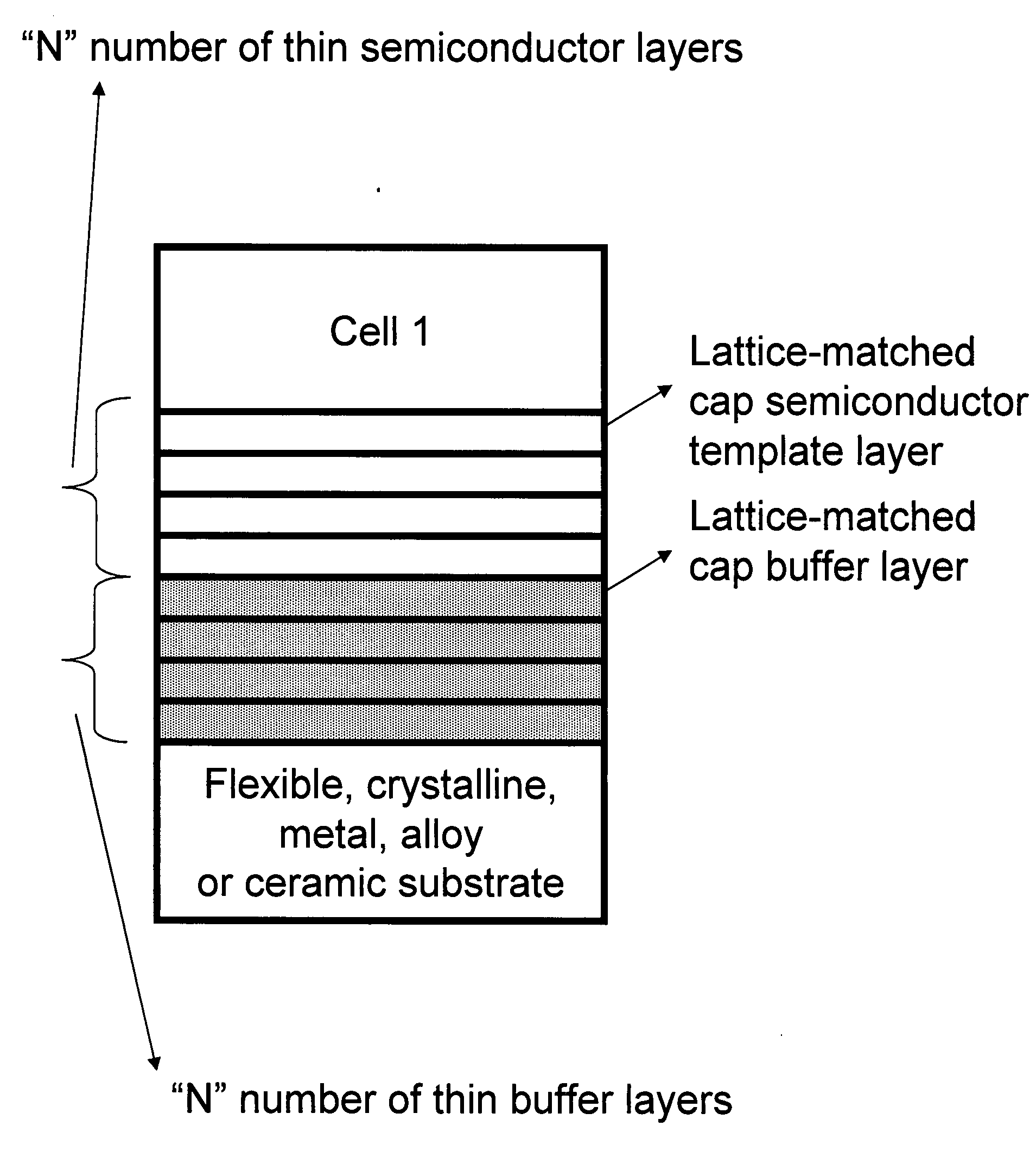
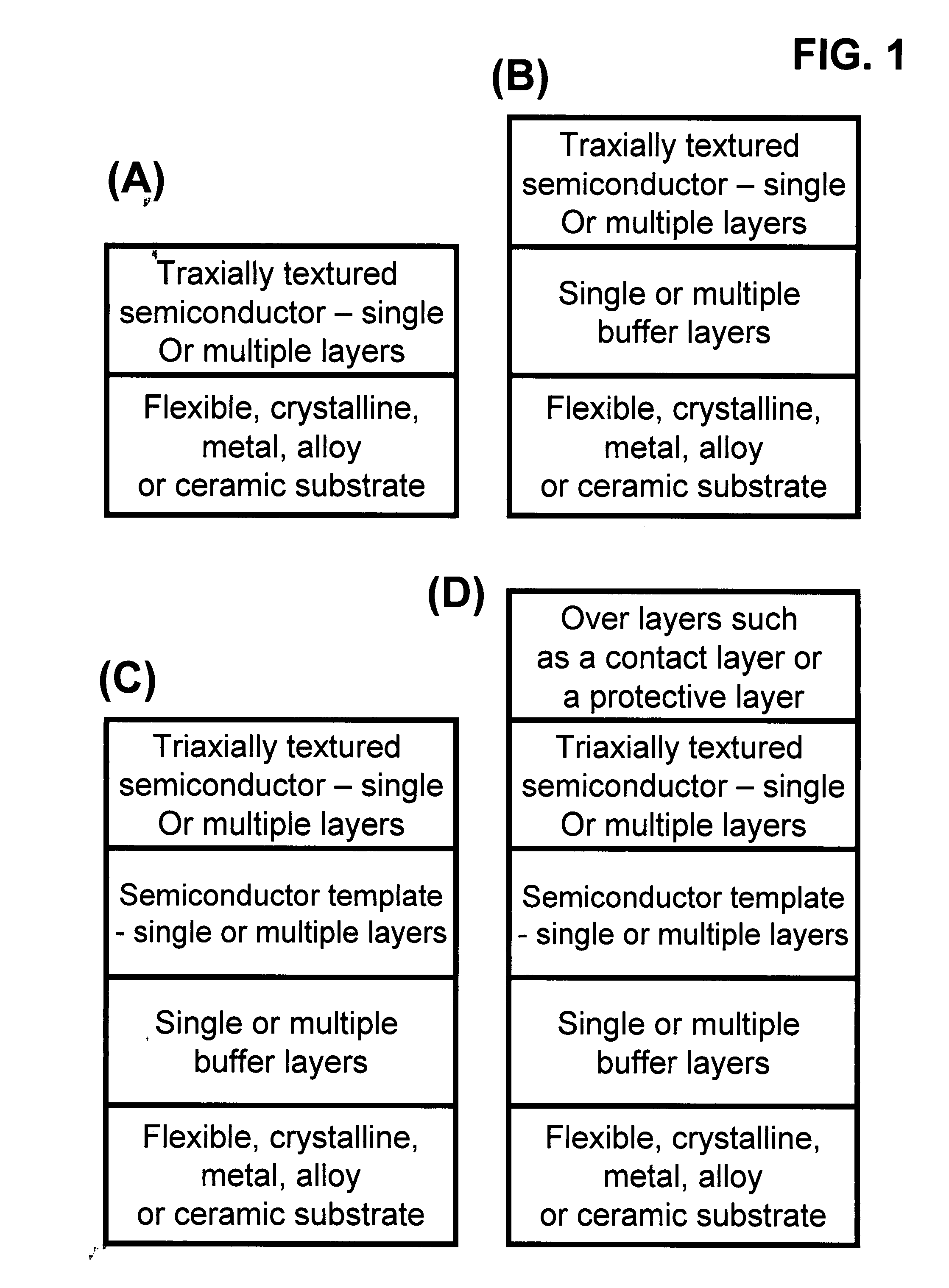
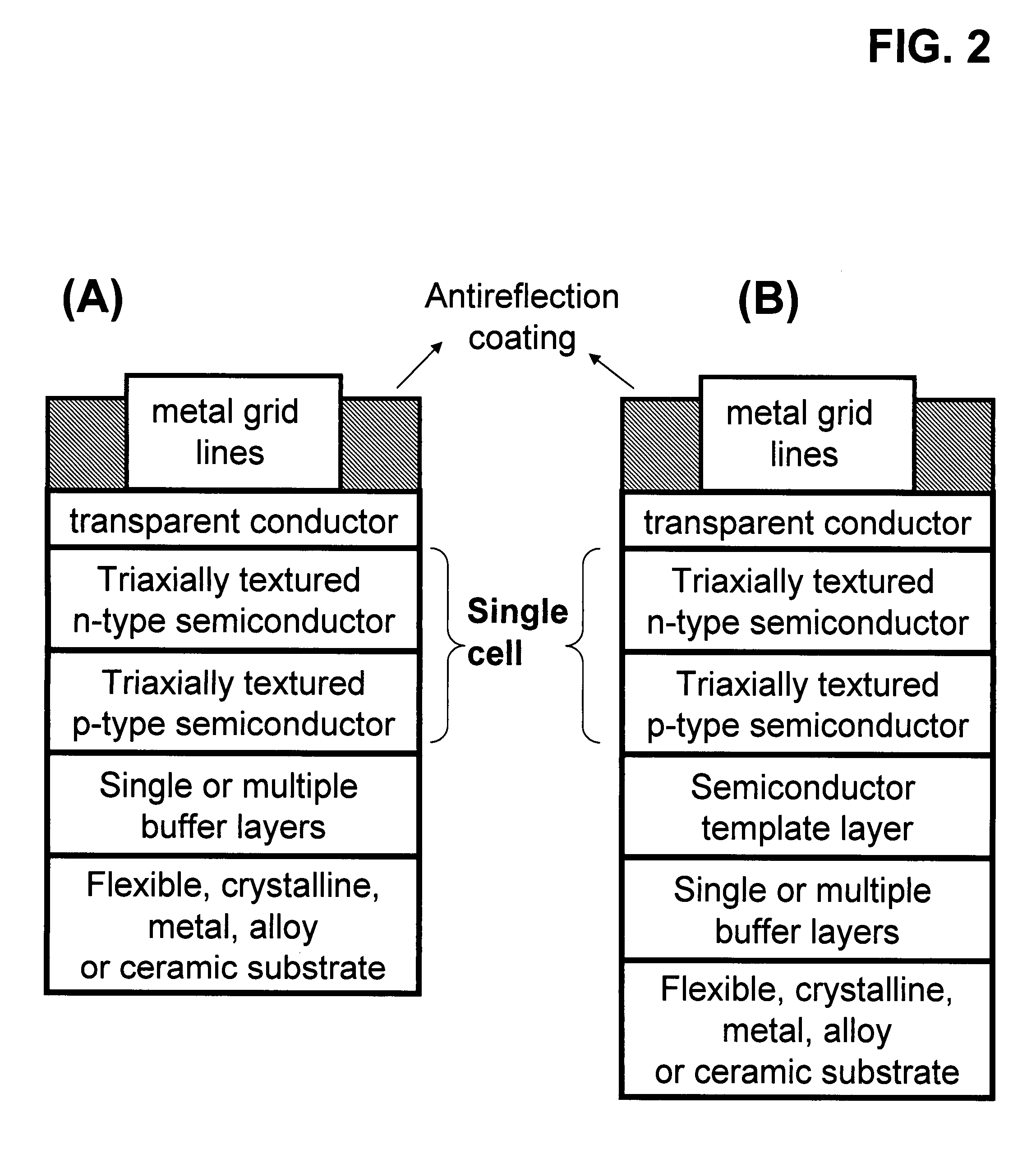
[0154]Shown in FIG. 14 is an idealized schematic representation in cross-section of a triaxially textured, flexible NiW alloy with a triaxially textured Si semiconductor layer on top of it with an intervening triaxially textured buffer layer of TiN.

[0155]This device is consistent with the devices depicted in FIG. 12. Biaxially textured Ni-3at % W was prepared by successive rolling of a powder metallurgy derived alloy coil from about 120 mils to a foil of about 2 mils or 50 microns in thickness. As-rolled crystallographic texture of the foil or tape was the standard Cu-type rolling texture of heavily deformed FCC metals. After the tape was degreased and dried, it was loaded into a reel-to-reel high vacuum (10−8 Torr) chamber, which contained a radio frequency induction heated furnace. The tape was pulled through the hot zone of the furnace at a rate that heated each part to 1250° C. for twenty minutes with a partial pressure of hydrogen sulfide gas of ˜3×10⁻⁷ Torr in order to form a ...

example 2

[0166]Starting with a biaxially textured, Ni-3at % W substrate, a 75 nm thick, epitaxial layer of γ-Al2O3 is grown by electron beam evaporation at a substrate temperature in the range of 700-850° C. This is followed by deposition of an epitaxial Si layer using chemical vapor deposition in the temperature range of 500-900° C. Numerous reports exist in the literature of epitaxial growth of Si on γ-Al2O3 see for example, Liwen tan, Qiyuan Wang, Jun Wang, Yuanhuan Yu, Zhongli Liu and Lanying Lin, “Fabrication of novel double-hetero-epitaxial SOI structure Si / γ-Al2O3 / Si,” Journal of Crystal Growth, vol. 247, pp. 255-260, 2003; K. Sawada, M. Ishida, T. Nakamura and N. Ohtake, “Metalorganic molecular beam epitaxy of films on si at low growth temperatures,” Appl. Phys. Lett., vol. 52, pp. 1672-1674, 1988; M. Shahjahan, Y. Koji, K. Sawada and M. Ishida, “Fabrication of resonance tunnel diode by gamma-Al2O3 / Si multiple heterostructures,” Japn. J. of Appl. Phys. Part 1, vol. 41 (4B), pp. 2602-...

example 3

[0167]Starting with a biaxially textured, Ni-3at % W substrate, a 75 nm thick Y2O3 layer is deposited epitaxially on NiW substrate using electron beam evaporation at a substrate temperature in the range of 300-700° C. This is followed by deposition of a 50 nm thick, epitaxial layer of γ-Al2O3 by electron beam evaporation at a substrate temperature in the range of 700-850° C. This is followed by deposition of an epitaxial Si layer using chemical vapor deposition in the temperature range of 500-900° C.


PUM

PropertyMeasurementUnit
Angleaaaaaaaaaa
Angleaaaaaaaaaa
Lengthaaaaaaaaaa

Abstract

Novel articles and methods to fabricate the same resulting in flexible, large-area, triaxially textured, single-crystal or single-crystal-like, semiconductor-based, electronic devices are disclosed. Potential applications of resulting articles are in areas of photovoltaic devices, flat-panel displays, thermophotovoltaic devices, ferroelectric devices, light emitting diode devices, computer hard disc drive devices, magnetoresistance based devices, photoluminescence based devices, non-volatile memory devices, dielectric devices, thermoelectric devices and quantum dot laser devices.

Description

STATEMENT REGARDING FEDERALLY FUNDED RESEARCH OR DEVELOPMENT[0001]This invention was made with Government support under Contract No. DE-AC05-000R22725 awarded by the United States Department of Energy. The Government has certain rights in this inventionFIELD OF THE INVENTION[0002]The invention relates to fabrication of high performance electronic devices comprising various types of semiconductors and articles made therefrom.BACKGROUND OF THE INVENTION[0003]Electronic devices based on semiconductors such as diodes, transistors and integrated circuits can be found everywhere in our daily lives, in televisions, automobiles, household gadgets and computers. We have come to rely on them and increasingly have come to expect higher performance at a lower cost. Personal computers clearly illustrate this trend. A significant factor in the successful growth of the computer industry is that through technological advances, smaller and smaller transistors were fabricated and more of them could b...

Claims


Application Information

Patent Timeline
IPC IPC(8): H01L29/04
CPCH01L21/0237H01L21/02488H01L21/02491H01L21/02521Y02E10/50H01L21/02609H01L31/036H01L31/0392H01L21/02568H01L31/03923H01L31/03925H01L31/03926Y02E10/541Y02P70/50
Inventor GOYAL, AMIT
Owner GOYAL AMIT
Why Eureka
Try Eureka