Method for manufacturing semiconductor substrate

a manufacturing method and semiconductor technology, applied in semiconductor/solid-state device manufacturing, basic electric elements, electric devices, etc., can solve the problem of difficult to obtain a silicon layer with a desired thickness, and achieve the effects of high bond strength, reduced ion irradiation depth, and high planarity

Inactive Publication Date: 2008-10-09
SEMICON ENERGY LAB CO LTD
View PDF39 Cites 31 Cited by
  • Summary
  • Abstract
  • Description
  • Claims
  • Application Information

AI Technical Summary

Benefits of technology

[0014]A barrier layer is preferably provided over a substrate having an insulating surface or an insulating substrate to which an SOI layer is bonded. Owing to the barrier layer, the single crystal semiconductor layer can be prevented from being contaminated.
[0015]By irradiation of a single crystal semiconductor substrate with one kind of ions selected from inert gas ions, halogen ions, or H3+ ions, variation of depths of ion irradiation is reduced, and an SOI substrate having a silicon layer with a desired thickness can be obtained.
[0016]When a single crystal semiconductor layer that is separated from a single crystal semiconductor substrate is bonded to a substrate serving as a base, the bond can be formed at a temperature of 700° C. or lower by the use of a silicon oxide film having a hydrophilic surface and high planarity, and including hydrogen. According to this structure, even when a substrate with an upper temperature limit of 700° C. or lower, such as a glass substrate, is used, a single crystal semiconductor layer provided with a bonding portion with high bond strength can be obtained.

Problems solved by technology

Therefore, the thickness of the silicon layer depends on the depth of ion irradiation, and thus, it is difficult to obtain a silicon layer with a desired thickness if the depths of ion irradiation vary.

Method used


Image

  • Method for manufacturing semiconductor substrate
  • Method for manufacturing semiconductor substrate
  • Method for manufacturing semiconductor substrate

Examples


embodiment mode 1

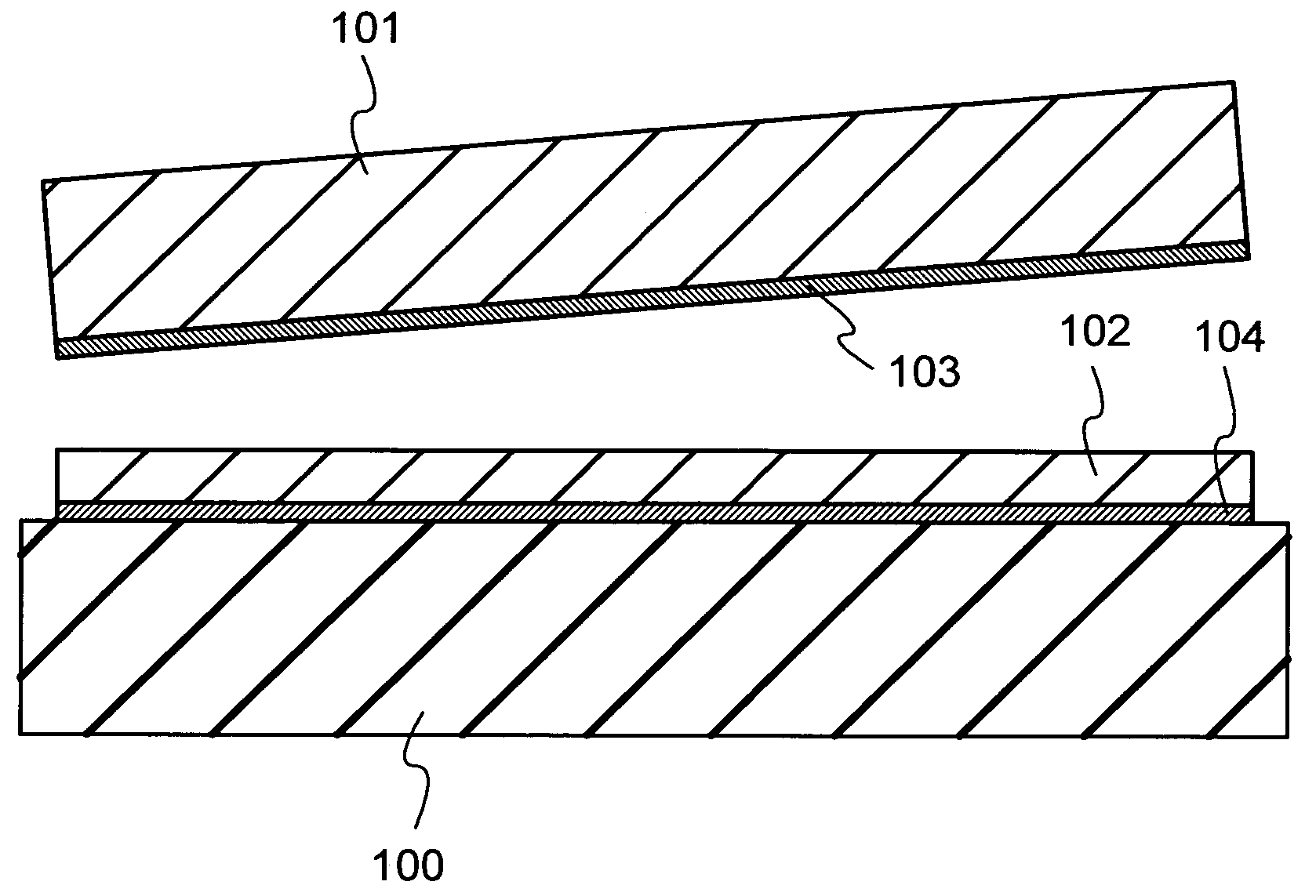
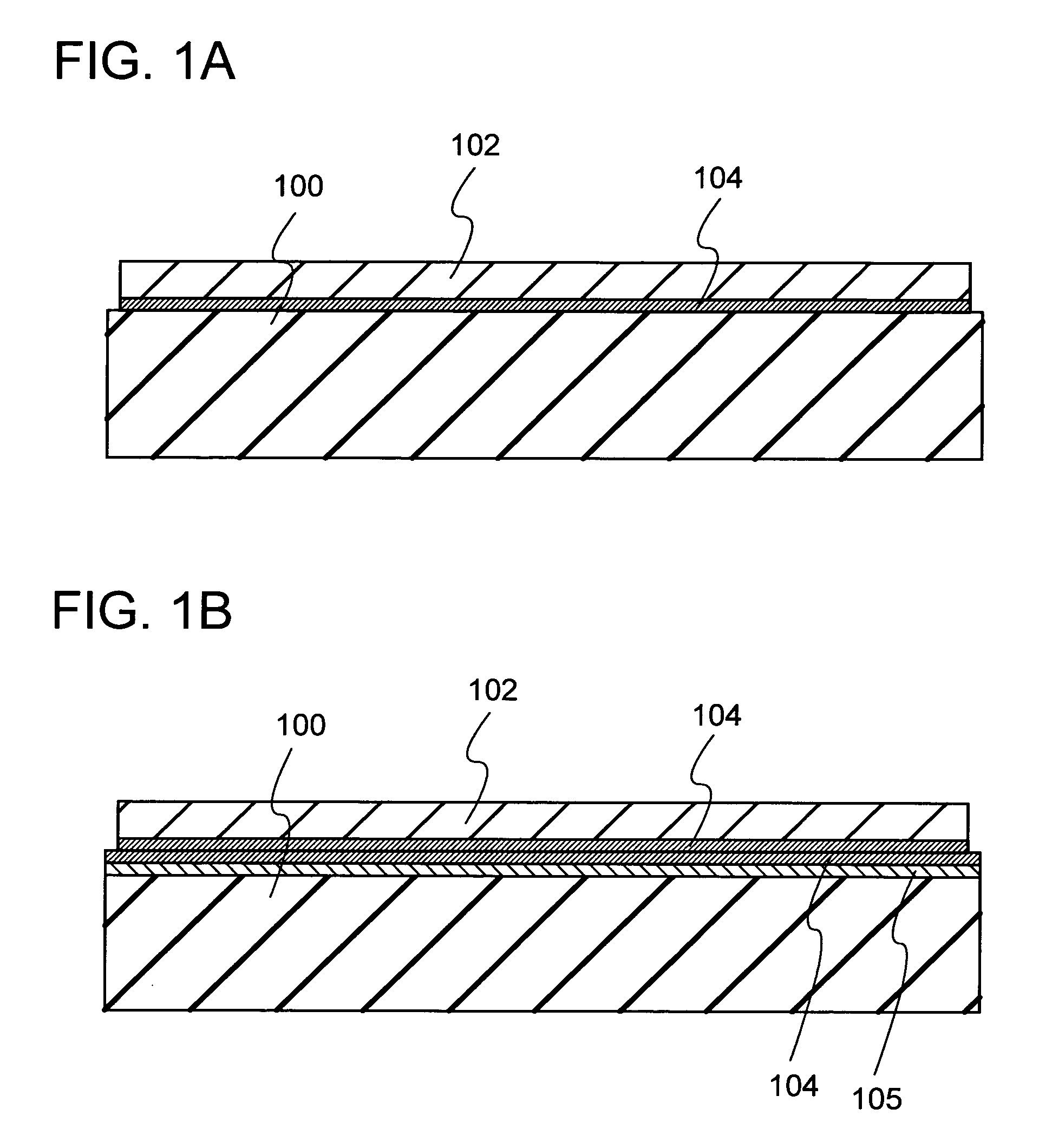
[0030]Each of FIGS. 1A and 1B shows a semiconductor substrate formed according to the present invention. In FIG. 1A, a base substrate 100 is a substrate having an insulating surface or an insulating substrate, and any of a variety of glass substrates that are used in the electronics industry, such as aluminosilicate glass substrates, aluminoborosilicate glass substrates, and barium borosilicate glass substrates, can be used. Alternatively, a quartz glass substrate or a semiconductor substrate such as a silicon wafer can be used. A single crystal semiconductor layer 102 is formed from a single crystal semiconductor, and single crystal silicon is typically used. Alternatively, a crystalline semiconductor layer formed from silicon, germanium, or a compound semiconductor such as gallium arsenide or indium phosphide which can be separated from a single crystal semiconductor substrate or a polycrystalline semiconductor substrate by a hydrogen ion implantation separation method, for exampl...

embodiment mode 2

[0041]This embodiment mode describes a method for manufacturing a semiconductor substrate described in Embodiment Mode 1 with reference to FIGS. 3A to 3C and FIG. 4.

[0042]A semiconductor substrate 101 shown in FIG. 3A is cleaned, and the semiconductor substrate 101 is irradiated with ions having equal mass that are accelerated by an electric field from a surface thereof to form an embrittlement layer 103 in the semiconductor substrate 101 at a predetermined depth. In this embodiment mode, ions of a halogen atom (also referred to as halogen ions) which had been subjected to mass separation are used. The halogen ions which had been subjected to mass separation are obtained by subjecting the material (mainly gas) including a halogen atom to mass separation. The ion irradiation is carried out in consideration of the thickness of a single crystal semiconductor layer that is to be transferred to the base substrate. A thickness of the single crystal semiconductor layer is set to be 5 to 50...

embodiment mode 3

[0055]This embodiment mode describes another mode of a method for manufacturing a semiconductor substrate which is described in Embodiment Mode 2.

[0056]In this embodiment mode, a semiconductor substrate 101 is irradiated with inert gas ions that are accelerated by an electric field instead of the halogen ions in Embodiment Mode 2, from a surface of the semiconductor substrate 101 as shown in FIG. 3A to form an embrittlement layer 103 in the semiconductor substrate 101 at a predetermined depth. It is to be noted that the inert gas ions are obtained by using a gas including an inert atom, and are referred to as inert ions or inert atom ions. The ion irradiation is carried out in consideration of the thickness of an LTSS layer that is to be transferred to a base substrate. A thickness of the LTSS layer is set to be 5 to 500 nm, preferably 10 to 200 nm. An accelerating voltage in irradiating the semiconductor substrate 101 with inert gas ions is set in consideration of such a thickness....


PUM


Abstract

A method for manufacturing a semiconductor substrate is provided, which comprises a step of irradiating a single crystal semiconductor substrate with ions to form an embrittlement layer in the single crystal semiconductor substrate, a step of forming a silicon oxide film over the single crystal semiconductor substrate, a step of bonding the single crystal semiconductor substrate and a substrate having an insulating surface with the silicon oxide film interposed therebetween, a step of performing a thermal treatment, and a step of separating the single crystal semiconductor substrate with a single crystal semiconductor layer left over the substrate having the insulating surface.

Description

BACKGROUND OF THE INVENTION[0001]1. Field of the Invention[0002]The present invention relates to a method for manufacturing a semiconductor substrate. In particular, the present invention relates to a semiconductor substrate in which a single crystal semiconductor layer or a polycrystalline semiconductor layer is bonded to a substrate having an insulating surface such as glass, and a semiconductor device.[0003]2. Description of the Related Art[0004]Integrated circuits have been developed, which use a semiconductor substrate called a silicon-on-insulator (SOI) substrate that has a thin single crystal semiconductor layer over an insulating surface, instead of a silicon wafer that is manufactured by thinly slicing an ingot of a single crystal semiconductor. An integrated circuit using an SOI substrate has been attracting attention because parasitic capacitance between drains of the transistors and the substrate is reduced and a semiconductor integrated circuit is made to have higher pe...

Claims


Application Information

Patent Timeline
Patent Type & Authority Applications(United States)
IPC IPC(8): H01L21/782
CPCH01L21/02164H01L21/02271H01L21/0234H01L21/3121H01L21/31612H01L21/76254H01L21/84
Inventor YAMAZAKI, SHUNPEI
Owner SEMICON ENERGY LAB CO LTD
Why Eureka
Try Eureka