
Optical Sensor For Extreme Environments

a technology of optical sensors and hazardous environments, applied in the field of optical sensors, can solve the problems of limited life-time, huge engineering challenge in realizing a sensor for such hazardous environments, and the production of chemically hazardous environments in coal and gas fired power systems, and achieves low cost, low loss, and high sensing resolution.

Inactive Publication Date: 2008-12-04
NUSENSORS +2
View PDF3 Cites 112 Cited by
  • Summary
  • Abstract
  • Description
  • Claims
  • Application Information

AI Technical Summary

Benefits of technology

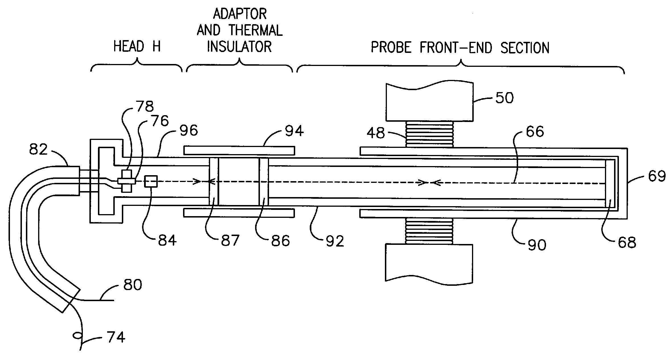
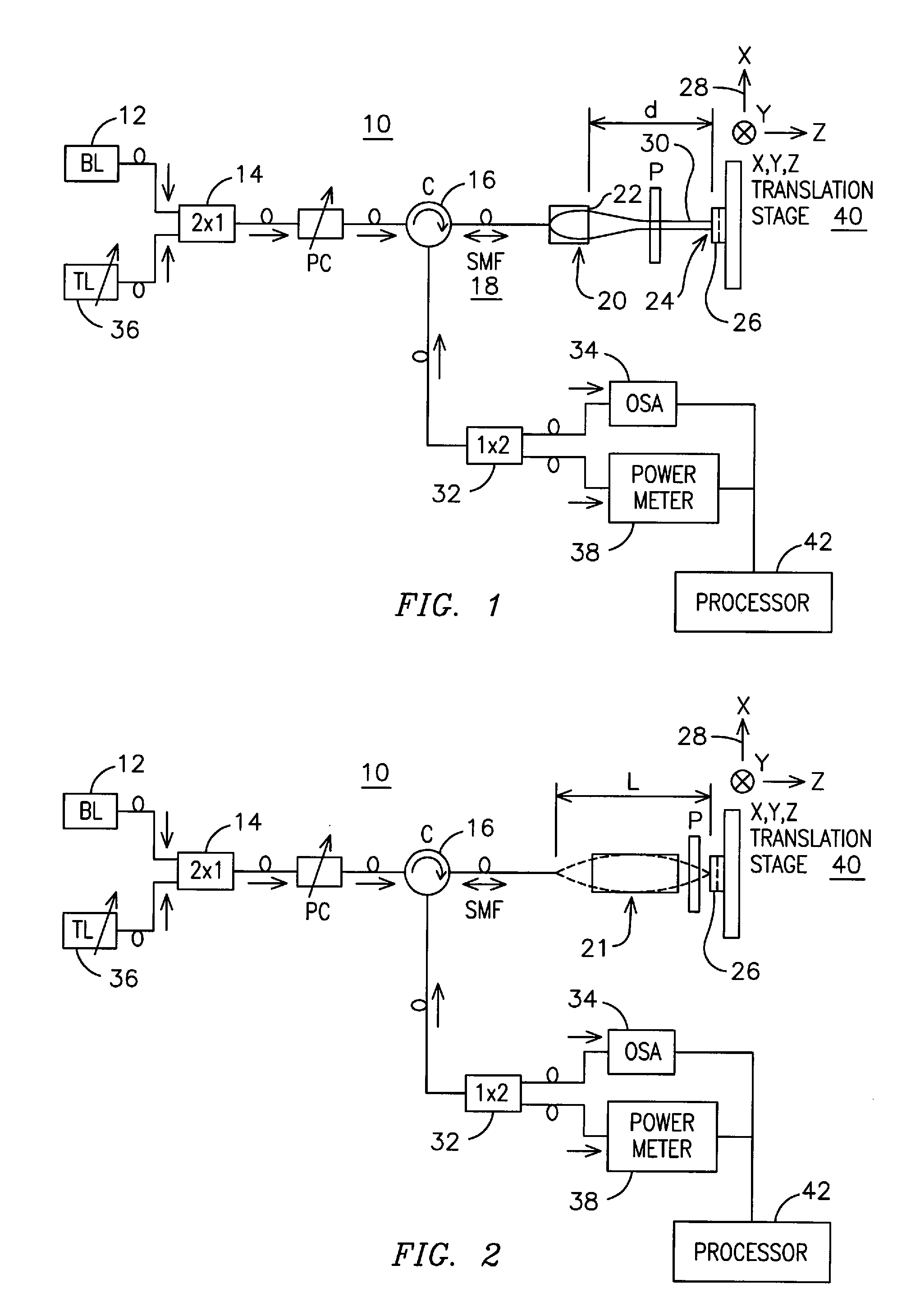
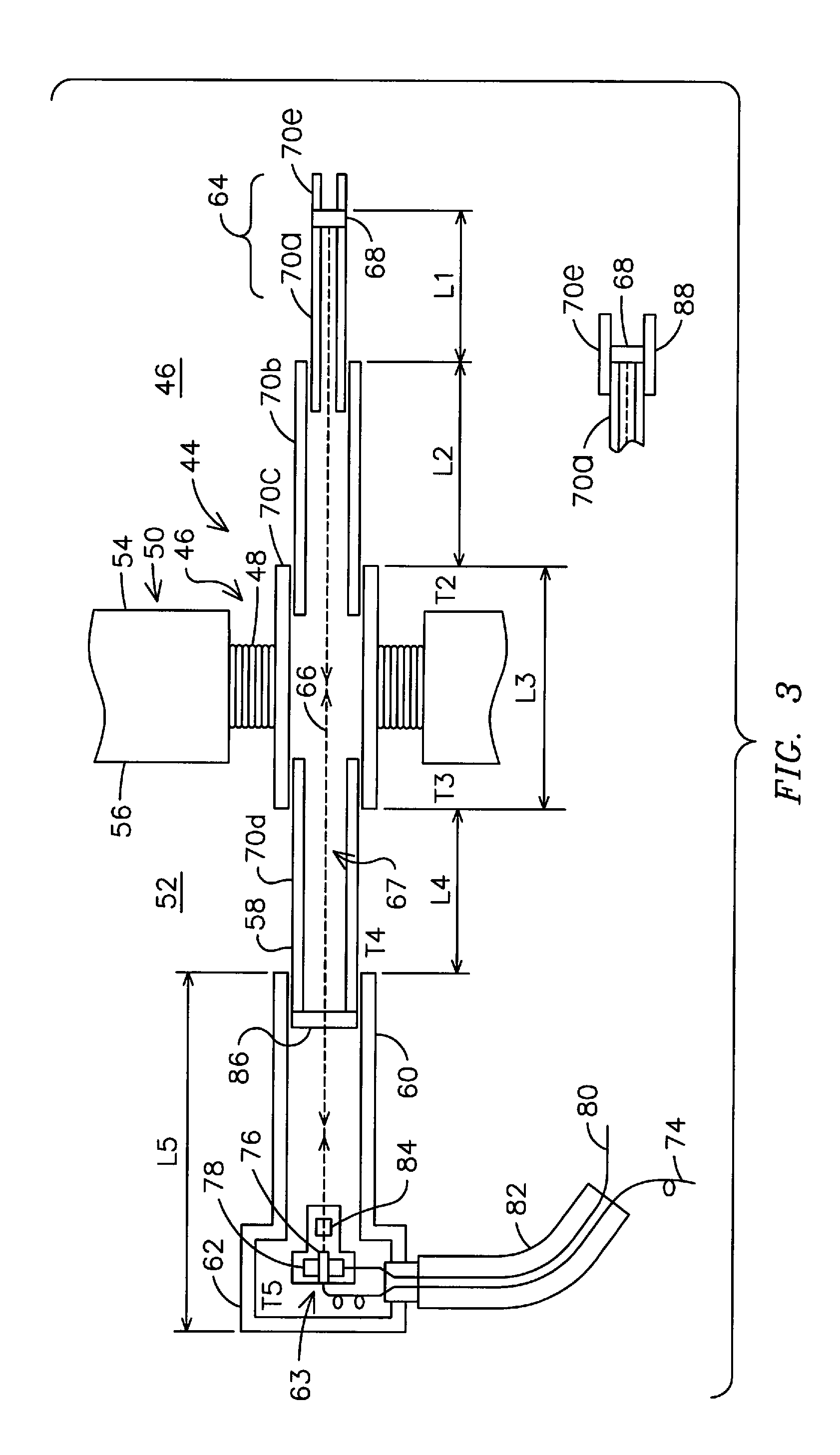
[0009]Ideally, one would like a robust optical sensor that can be remoted, is minimally invasive, works at high temperatures (e.g., 2000° C.) and pressures including chemically corrosive environments, requires low cost low loss optics, has high sensing resolution over any extended wide unambiguous range, and provides easy access to many sensing points. In commonly assigned U.S. patent application Ser. No. 11 / 185,540 incorporated herein by reference, modules for the needed extreme environment minimally invasive optical free-space laser beam targeted optical sensor using preferably single crystal Silicon Carbide (SiC) optical sensor chip(s) acting as a natural Fabry-Perot Etalon(s) are described. A key point in these designs is that laser light is launched into freespace using a Single-Mode Fiber (SMF); hence the light beam striking the temperature sensing SiC crystal has excellent spatial coherence (or collimation properties), making the optically sensed reading highly accurate and sensitive. The present application describes robust optical probe designs for these earlier described SiC single crystal optical sensors, including novel techniques for measurement of refractive index, temperature, pressure, and thickness.
[0011]Mechanical motion of alignment mirrors have been described to keep the freespace laser beam targeting on the SiC chip and receive optical detector. In the present application, described is a simpler non-mirror electronically actuated mechanical alignment assembly technique for the SMF-Lens combination so the sensor probe can implement fast real-time alignment operations for the free-space beam striking the sensing SiC single crystal that is acting as a temperature sensor. In other words, using for example fine tilt control piezo-electric motion control mechanics on the entire SMF-Fiber lens (FL) assembly, one can accurate point the laser beam (LB) to the correct retroreflective position on the SiC chip, thus enabling robust temperature probe design in harsh environments.
[0018]An optical pressure sensor can be designed when using a High Pressure Capsule (HPC) design where the HPC uses the single crystal SiC chip as an optical window accessed by a laser beam. The HPC can be made with the sintered SiC material so CTE's of chip / window and HPC material are matched to prevent thermal deformation effects on the chip. The sensors can also be designed into small fiber-optic packages.

Problems solved by technology

Realizing a sensor for such hazardous environments remains to be a tremendous engineering challenge.
In addition, coal and gas fired power systems produce chemically hazardous environments with chemical constituents and mixtures containing for example carbon monoxide, carbon dioxide, nitrogen, oxygen, sulphur, sodium, and sulphuric acid.
Over the years, engineers have worked very hard in developing electrical high temperature sensors (e.g., thermo-couples using platinum and rodium), but these have shown limited life-times due to the wear and tear and corrosion suffered in power plants [R. E. Bentley, “Thermocouple materials and their properties,” Chap.
The single crystal Sapphire fiber FBG has a very large diameter (e.g., 150 microns) that introduces multi-mode light propagation noise that limits sensor performance.
Hence this described sensor frontend sensing element not only has low optical efficiency and high noise generation issues due to its multi-mode versus SMF design, the sensor frontend is limited by the lowest high temperature performance of a given component in the assembly and not just by the Sapphire crystal and zirconia high temperature ability.
In particular, the Sapphire Crystal is highly birefringent and hence polarization direction and optical alignment issues become critical.
Hence this temperature sensor design is again limited by the spectral spoiling plus other key effects when using very broadband light with MMFs.
Specifically, light exiting a MMF with the collimation lens has poor collimation as it travels a free-space path to strike the sensing crystal.
This all leads to additional coupling problems for the receive light to be picked up by the six MMFs engaged with the single fixed collimation lens.
Another problem plaguing this design is that any unwanted mechanical motion of any of the mechanics and optics along the relatively long (e.g., 1 m) freespace optical processing path from seven fiber-port to Sapphire crystal cannot be countered as all optics are fixed during operations.
Hence, this probe can suffer catastrophic light targeting and receive coupling failure causing in-operation of the sensor.
Although this design used two sets of manual adjustment mechanical screws each for 6-dimension motion control of the polarizer and collimator lens, this manual alignment is only temporary during the packaging stage and not during sensing operations.
Thus, this mentioned design is not a robust sensor probe design when using freespace optics and fiber-optics.
19-26, 2004.) have used the Sapphire MMF in contact with a high temperature handling optical crystal (e.g., Sapphire) to realize a temperature sensor, but again the limitations due to the use of the MMF are inherent to the design.
In particular, high temperature gradients and fast temperature / pressure temporal effects can cause stress fields at the SiC thin film-Sapphire interface causing deterioration of optical properties (e.g., interface reflectivity) required to form a quality Fabry-Perot etalon needed for sensing based on SiC film refractive index change.
Note that these previous works also had a limitation on the measured unambiguous sensing (e.g., temperature) range dictated only by the SiC thin film etalon design, i.e., film thickness and reflective interface refractive indices / reflectivities.
But making a thinner SiC film makes the sensor less sensitive and more fragile to pressure.
In addition, temperature change is preferably estimated based on tracking optical spectrum minima shifts using precision optical spectrum analysis optics, making precise temperature estimation a challenge dependent on the precision (wavelength resolution) of the optical spectrum analysis hardware.
Hence there exists a dilemma where a thick film is desired for better sensing resolution but it requires a better precision optical spectrum analyzer (OSA) and of course thicker thin film SiC etalons are harder to make optically flat.
Finally, all to these issues the Fabry-Perot cavity spectral notch / peak shape spoiling due to varying cavity material parameters that in-turn leads to deterioration in sensing resolution.
These methods are not effective to form a real-time temperature sensor as these prior-art methods require the knowledge of the initial temperature when fringe counting begins.
For industrial power plant applications, such a prior knowledge is not possible, while for laboratory material growth and characterization, this a prior knowledge is possible.

Method used


Image

  • Optical Sensor For Extreme Environments
  • Optical Sensor For Extreme Environments
  • Optical Sensor For Extreme Environments

Examples


Embodiment Construction

[0032]Knowing the exact thickness of optical components is a critical need when designing high quality large, miniature, and super small optics for numerous platforms such as integrated-waveguide optics, bulk-optics, and fiber-optics. Over the years, many methods have been described to measure thickness from the thin-film level (i.e., smaller than the optical wavelength) to thick plates (i.e., hundreds of wavelengths). Perhaps the most tried method is based on the classic Michelson optical interferometry using a broadband optical source such as white light [see P. A. Flourney, R. W. McClure, G. Wyntjes, “White light interferometric thickness gauge,” Appl. Opt., 11, 1907 (1972); L. M. Smith and C. C. Dobson, “Absolute displacement measurements using modulation of the spectrum of white light in a Michelson interferometer,” Appl. Opt., 28, 3339 (1989)]. Here, the short coherence length of the broadband source is used to produce interferometer arms path-length difference-based output de...


PUM


Abstract

An optical sensing probe includes a tube having a tip portion configured for placement in an environment in which conditions are to be sensed and an etalon having a known characteristic disposed proximate the tip portion. The tube also includes a head portion remote from the tip portion containing a light directing element for directing light beams at the etalon and receiving reflected light beams from the etalon wherein the received reflected light beams are used for determining an environmental condition proximate the tip portion. A method for measuring a thickness of the etalon may include directing a light beams at different frequencies at the etalon and receiving the light beams from the etalon. The method may also include identifying conditions of the respective light beams condition received from the etalon and then calculating a first thickness of the etalon responsive to the respective conditions and the known characteristic.

Description

SPECIFIC DATA RELATED TO INVENTION[0001]This application claims the benefit of U.S. provisional application No. 60 / 742,813 filed on Dec. 6, 2005.BACKGROUND OF INVENTION[0002]The present invention relates to optical sensors and, more particularly, to optical sensors using etalons for remote sensing in extreme environments.[0003]There are numerous vital sensing scenarios in commercial and defense sectors where the environment is extremely hazardous. Specifically, the hazards can be for instance due to extreme temperatures, extreme pressures, highly corrosive chemical content (liquids, gases, particulates), nuclear radiation, biological agents, and high Gravitational (G) forces. Realizing a sensor for such hazardous environments remains to be a tremendous engineering challenge. One specific application is fossil fuel fired power plants where temperatures in combustors and turbines typically have temperatures and pressures exceeding 1000° C. and 50 Atmospheres (atm). Future clean design...

Claims


Application Information

Patent Timeline
IPC IPC(8): G01B11/28G01B11/02
CPCG01B9/02004G01B9/02028G01B9/02056G01B9/0209G01B9/02023G01B2290/25G01B9/02072
Inventor RIZA, NABEEL AGHAPEREZ, FRANK
Owner NUSENSORS
Learn More