Group-III Nitride-Based Light Emitting Device

a light-emitting device and nitride-based technology, which is applied in semiconductor devices, semiconductor device details, electrical apparatus, etc., can solve the problems of poor electric characteristics of top-emission-type light-emitting diodes, poor current injection and current spreading, and poor nitride-based compatibility of spreading layers, etc., to improve the light transmittance of transparent electrodes, improve the ohmic contact characteristics, and improve the current-voltage characteristics

Active Publication Date: 2008-12-11
SAMSUNG DISPLAY CO LTD
View PDF2 Cites 44 Cited by
  • Summary
  • Abstract
  • Description
  • Claims
  • Application Information

AI Technical Summary

Benefits of technology

[0034]As mentioned above, thermally decomposed nitride having p-type nitride-based ohmic electrode characteristics is used as a p-type ohmic electrode of a group-III nitride-based light emitting diode.
[0035]Accordingly, the ohmic contact characteristics can be improved at the interfacial surface between the p-type o

Problems solved by technology

In addition, the top-emission type light emitting diode has poor electric characteristics, such as bad current injection and current spreading, derived from the characteristics of the p-type nitride-based cladding layer having a low hole carrier density value of 1018/cm3.
The p-type current spreading layer having low light transmittance absorbs most of light generated from the nitride-based light emitting diode, so the p-type current spreading layer is not suitable for the nitride-based light emitting diode having large capacity, large area and high brightness.
However, the high-reflective electrode material has a low work function value and creates new-phase nitride at an interfacial surface during the heat treatment process, so the p-type reflective ohmic contact layer 160 has a bad ohmic contact characteristic relative to the p-type nitride-based cladding layer 150 and represents bad mechanical adhesion and bad thermal stability, so that the life span of the semiconductor device is shortened and the productivity thereof is lowered.
However, the silver metal exhibits thermal instability, bad

Method used


Image

  • Group-III Nitride-Based Light Emitting Device
  • Group-III Nitride-Based Light Emitting Device
  • Group-III Nitride-Based Light Emitting Device

Examples


first embodiment

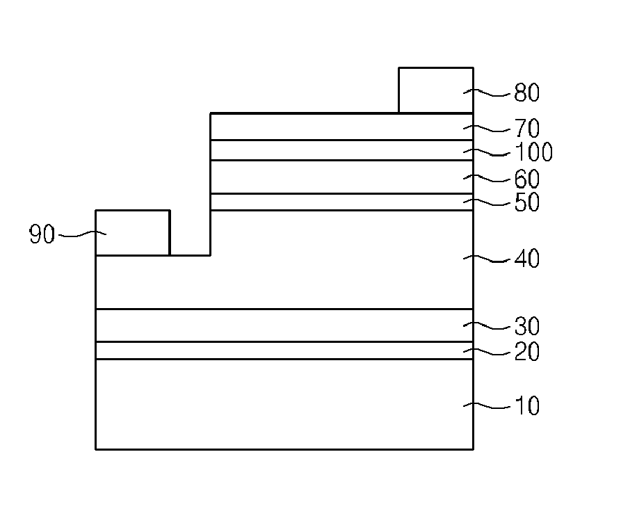
[0052]FIGS. 3 and 4 are sectional views showing a light emitting device employing a p-type multi-layered ohmic contact electrode structure according to the present invention.

[0053]In detail, FIG. 3 shows a group-III nitride-based top-emission type light emitting diode (TELED) employing an insulating growth substrate 10 including sapphire (Al2O3), and FIG. 4 shows a group-III nitride-based top-emission type light emitting diode (TELED) employing a conductive substrate 10 having a conductive material layer including silicon carbide (SiC), zinc oxide (ZnO), silicon (Si), gallium arsenic (GaAs), a metal, such as copper (Cu), nickel (Ni) or aluminum (Al), or an alloy formed through electroplating or a bonding transfer scheme disclosed in various documents.

[0054]Referring to FIG. 3, the group-III nitride-based TELED includes a substrate 10 on which a low-temperature nucleation layer 20, a nitride-based buffer layer 30, an n-type nitride-based cladding layer 40, a nitride-based active laye...

second embodiment

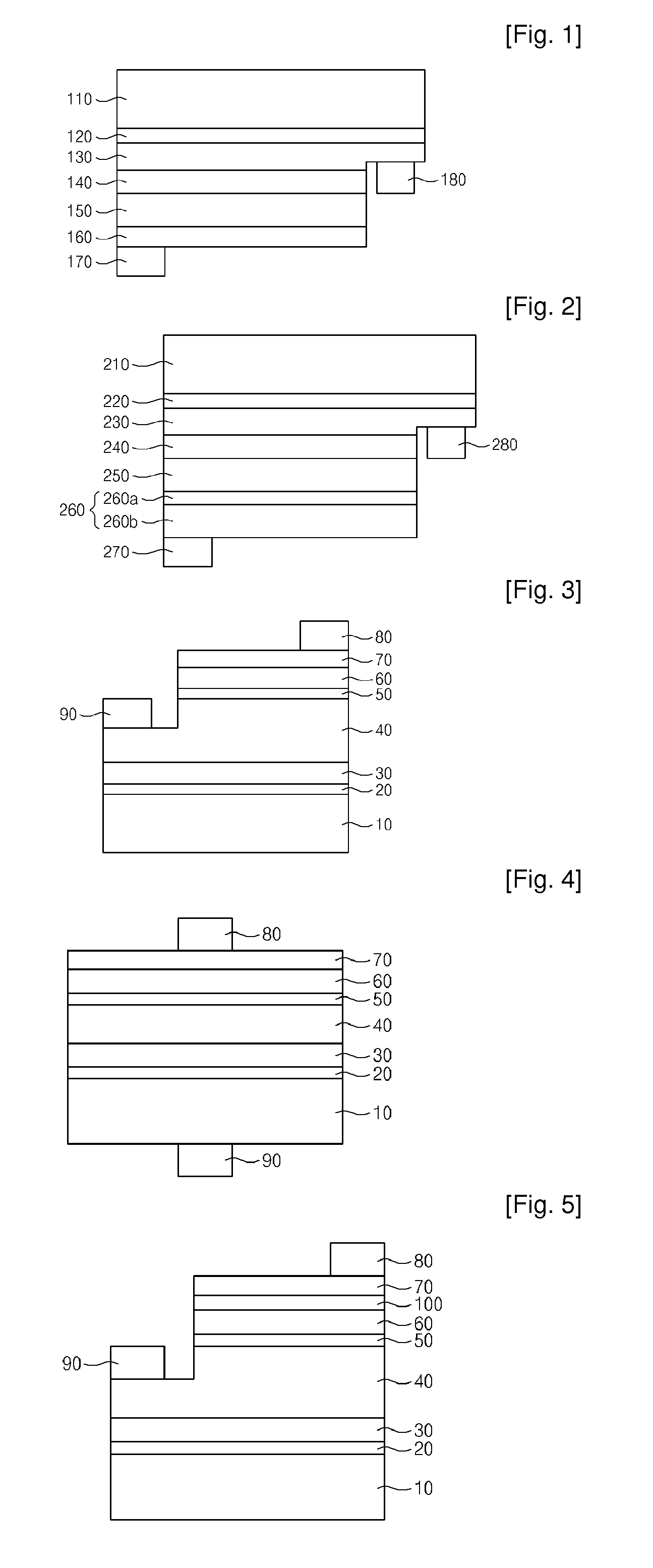
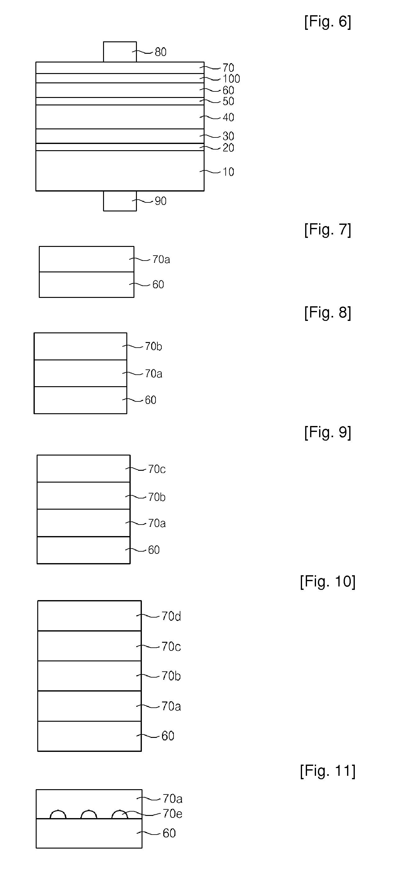
[0077]FIGS. 5 and 6 are sectional views showing a light emitting device employing a p-type multi-layered ohmic contact electrode structure according to the present invention. In FIGS. 5 and 6, the same reference numerals will be assigned to the elements having the same functions and structures as those shown in FIGS. 3 and 4 and detailed description thereof will be omitted in order to avoid redundancy.

[0078]In detail, FIG. 5 shows a group-III nitride-based top-emission type light emitting diode (TELED) employing an insulating growth substrate 10 including sapphire (Al2O3), and FIG. 6 shows a group-III nitride-based top-emission type light emitting diode (TELED) employing a conductive substrate 10 having a conductive material layer including silicon carbide (SiC), zinc oxide (ZnO), silicon (Si), gallium arsenic (GaAs), a metal, such as copper (Cu), nickel (Ni) or aluminum (Al), or an alloy formed through electroplating or a bonding transfer scheme disclosed in various documents.

[0079...

third embodiment

[0105]FIG. 15 is a sectional view showing a flip-chip type nitride-based light emitting device employing an ohmic modification layer according to the present invention.

[0106]Referring to FIG. 15, the p-type multi-layered reflective ohmic contact layer 360 includes an ohmic modification layer 360a and a reflective metal layer 360b which are sequentially stacked. The ohmic modification layer 360a includes the TCON.

[0107]The TCON used for the ohmic modification layer 360a basically includes at least one of indium (In), tin (Sn), zinc (Zn), cadmium (Cd), gallium (Ga), aluminum (Al), magnesium (Mg), titanium (Ti), molybdenum (Mo), nickel (Ni), copper (Cu), silver (Ag), gold (Au), platinum (Pt), rhodium (Rh), iridium (Ir), ruthenium (Ru), and palladium (Pd), combined with both oxygen (O) and nitrogen (N).

[0108]The reflective metal layer 360b includes at least one of aluminum (Al), silver (Ag), rhodium (Rh), palladium (Pd), nickel (Ni), gold (Au), and platinum (Pd). According to the presen...


PUM


Abstract

Disclosed is a group-III nitride-based light emitting diode. The group-III nitride-based light emitting diode includes a substrate, an n-type nitride-based cladding layer formed on the substrate, a nitride-based active layer formed on the n-type nitride-based cladding layer, a p-type nitride-based cladding layer formed on the nitride-based active layer, and a p-type multi-layered ohmic contact layer formed on the p-type nitride-based cladding layer and including thermally decomposed nitride. The thermally decomposed nitride is obtained by combining nitrogen (N) with at least one metal component selected from the group consisting of nickel (Ni), copper (Cu), zinc (Zn), indium (In) and tin (Sn). An ohmic contact characteristic is enhanced at the interfacial surface of the p-type nitride-based cladding layer of the group-III nitride-based light emitting device, thereby improving the current-voltage characteristics. In addition, since the light transmittance of the transparent electrode is improved, light efficiency and brightness of the group-III nitride-based light emitting device are also improved.

Description

TECHNICAL FIELD[0001]The present invention relates to a group-III nitride-based light emitting device. More particularly, the present invention relates to a group-III nitride-based light emitting device, capable of improving light emitting efficiency and expanding life span of semiconductor devices.BACKGROUND ART[0002]In order to realize light emitting devices, such as light emitting diodes or laser diodes using group-III nitride-based compound semiconductors including GaN semiconductors, the structure and characteristics of an ohmic contact electrode provided between a semiconductor and an electrode pad are very important.[0003]A currently available nitride-based light emitting device is formed on an insulating sapphire (Al2O3) substrate. Group-III nitride-based light emitting diodes formed on the insulating sapphire substrate are classified into top-emission type light emitting diodes and flip-chip type light emitting diodes.[0004]The group-III nitride-based top-emission type ligh...

Claims


Application Information

Patent Timeline
IPC IPC(8): H01L33/00H01L33/06H01L33/10H01L33/32H01L33/42
CPCH01L33/32H01L33/40H01L33/42
Inventor SEONG, TAE-YEON
Owner SAMSUNG DISPLAY CO LTD
Why Eureka
Try Eureka