Magnetic thin film, magnetoresistance effect device and magnetic device using the same

a technology of magnetoresistance effect and thin film, which is applied in the field of magnetic thin film, magnetoresistance effect device and magnetic device using the same, can solve the problems of insufficient tmr value, no reports that the so far fabricated thin film is a half metal, and inability to be practically used. to achieve the effect of high speed and large capacity

Inactive Publication Date: 2009-01-15
JAPAN SCI & TECH CORP
View PDF3 Cites 10 Cited by
  • Summary
  • Abstract
  • Description
  • Claims
  • Application Information

AI Technical Summary

Benefits of technology

[0034]In the constitution described above, a tunnel or a giant magnetoresistance effect device is preferably used in which a free layer is said Co2MGa1-xAlx (where 0≦x≦0.7) magnetic thin film. A tunnel or a giant magnetoresistance effect device may be used in which Co2MGa1-xAlx thin film is formed by heating a substrate at 500° C. or lower including non-heating, or by further annealing said formed thin film at 500° C. or lower. A tunnel or a giant magnetoresistance effect device may be used in which a buffer layer is provided between the substrate and Co2MGa1-xAlx thin film. A tunnel or a giant magnetoresistance effect device may be used in which the substrate is either one of thermally oxidized Si, glass, MgO single crystal, GaAs single crystal, or Al2O3 single crystal. A tunnel or a giant magnetoresistance effect device may be used in which the buffer layer is at least either one of Al, Cu, Cr, Fe, Nb, Ni, Ta, or NiFe.
[0035]According to the constitution described above, a magnetic head and a magnetic recording device of large capacity and high speed can be obtained by using a magnetoresistance effect device of large TMR or GMR in the low external magnetic field at room temperature.

Problems solved by technology

Therefore, though GMR effect devices of CIP structure have already been practically used for play back heads of hard discs, GMR effect devices of CPP structure have so far not been practically used.
However, MRAM has such a problem to be solved that, when a device size is made small for high density, the noise increases accompanying the non-homogeneity of devices, thereby the TMR value is currently insufficient.
However, there have been no reports that the so far fabricated thin film is a half metal.
The fabrication of tunnel junction devices using these half metals has been partly attempted, but TMR at room temperature is in all cases unexpectedly low, such that its maximum value is at most between 10 and 20% of the case using Fe3O4.
The tunnel junction in particular has difficulty to attain the half metal electronic state at its interface.
This is regarded as the cause for large TMR not attained.
From the above, there remains a problem that the fabrication of half metal thin film is actually very difficult, and the half metal thin film good enough to be used for various magnetoresistance effect devices has so far not been obtained.
However, since the CoAl compound of B2 structure is extremely stable at Co2CrAl side where x=0, there is such a problem that CoAl of B2 structure and CoCr of A2 structure tend to cause two phase separation, thereby such a single phase alloy as Co2Fe0.4Cr0.6Al thin film which is expected to have half metal characteristics is hard to obtain.

Method used


Image

  • Magnetic thin film, magnetoresistance effect device and magnetic device using the same
  • Magnetic thin film, magnetoresistance effect device and magnetic device using the same
  • Magnetic thin film, magnetoresistance effect device and magnetic device using the same

Examples


example 1

[0091]Examples of the present invention are explained hereafter.

[0092]As the magnetic thin film of the present invention Co2MGa1-xAlx, Co2CrGa was fabricated with Cr as M and composition x=0. In this case, the average valence electron concentration Z in M is 6.

[0093]The fabrication of the alloy Co2CrGa as the material of the magnetic thin film of the present invention will be explained first. Co, Cr, and Ga of high purity were input into an arc melting apparatus by the composition ratio of 25%, 25%, and 50%, respectively, melted at 1100° C. for 24 hours, and hardened in ice water to fabricate Co2CrGa alloy.

[0094]FIG. 10 is a view illustrating electron beam diffraction of [01-1] incoming radiation of Co2CrGa alloy prepared in Example 1. The acceleration voltage of electron beam was 200 kV, and the numbers in the figure show diffraction from (200), (111), and (022) planes, respectively. As is obvious from the figure, both regular reflections from (200) and (111) planes appeared, and t...

example 2

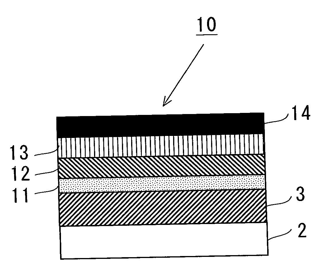
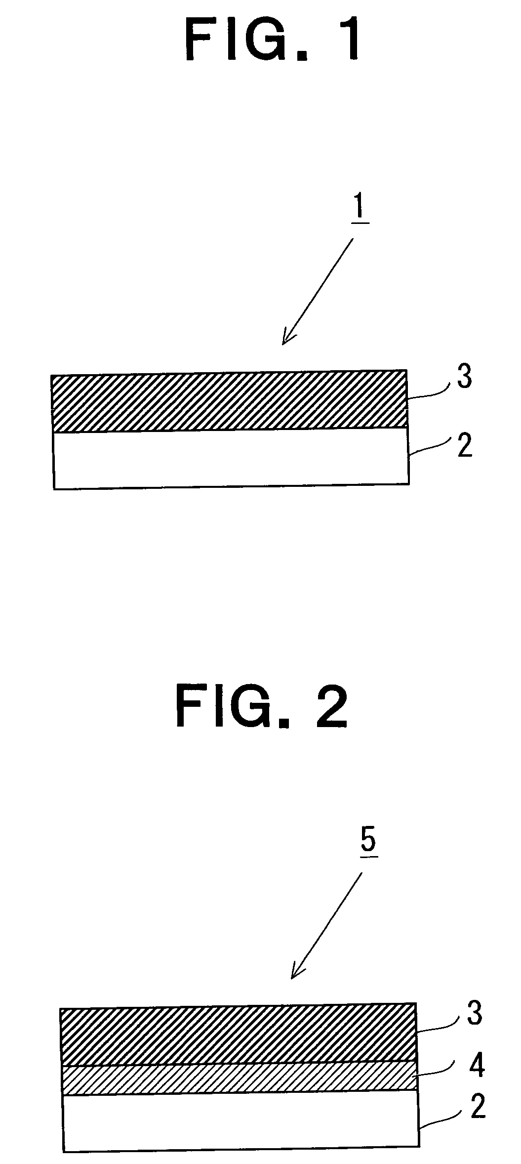
[0096]The tunnel magnetoresistance effect device 15 of the spin valve type as shown in FIG. 5 was fabricated at room temperature. The tunnel magnetoresistance effect device 15 was fabricated by using a magnetron sputtering apparatus and a metal mask, with Ta as a buffer layer 4, and sequentially depositing Ta (10 nm) / Co2CrGa (300 nm) / AlOx (1.6 nm) / Co90Fe10 (10 nm) / NiFe (2 nm) / IrMn (20 nm) / Ta (10 nm) onto the thermally oxidized Si substrate 2. The numbers in parentheses are respective film thicknesses. Ta is the buffer layer 4, Co2CrGa thin film 3 is the ferromagnetic free layer, AlOx is the tunnel insulation layer 11, Co90Fe10 and NiFe are ferromagnets comprising a complex film made of pin layers of the ferromagnetic layer 12, IrMn is the antiferromagnetic layer 13 and has a role to fix the spins of the ferromagnetic layer 12 of Co90Fe10 / NiFe. Ta on IrMn as the antiferromagnetic layer 13 is the protective layer 14.

[0097]The high frequency power of the magnetron was 100 W for respect...

example 3

[0099]The tunnel magnetoresistance effect device 15 of the same spin valve type as Example 2 was fabricated by using Co2CrGa thin film 3 except that its film thickness was 100 nm. By applying the external magnetic field to said tunnel magnetoresistance effect device 15, the magnetoresistance was measured at room temperature. FIG. 12 is a view illustrating the magnetic field dependency of the resistance of the tunnel magnetoresistance effect device 15 of Example 3. The abscissa of the figure shows the external magnetic field H (Oe), and the ordinate shows the resistance (Ω). The magnetoresistance including also its hysteresis characteristics was measured by sweeping the external magnetic field. Hereby, the TMR was determined as 3.2%.

[0100]In Examples 2 and 3, no plateau was seen in TMR curves, and the perfect antiparallel state of spins was not realized. By optimizing the fabrication conditions of the tunnel magnetoresistance effect device 15, a TMR will be made dramatically larger.


PUM

PropertyMeasurementUnit
thicknessaaaaaaaaaa
temperatureaaaaaaaaaa
electrical resistivityaaaaaaaaaa

Abstract

Magnetic thin film having high spin polarizability and a magnetoresistance effect device and a magnetic device using the same, provided with a substrate (2) and Co2MGa1-xAlx thin film (3) formed on the substrate (2), the Co2MGa1-xAlx thin film (3) has a L21 or B2 single phase structure, M of the thin film is either one or two or more of Ti, V, Mo, W, Cr, Mn, and Fe, an average valence electron concentration Z in M is 5.5≦Z≦7.5, and 0≦x≦0.7, shows ferromagnetism at room temperature, and can attain high spin polarizability. A buffer layer (4) may be inserted between the substrate (2) and the Co2FexCr1-xAl thin film (3). The tunnel magnetoresistance effect device and the giant magnetoresistance effect device using this magnetic thin film can attain large TMR and GMR at room temperature under the low magnetic field.

Description

TECHNICAL FIELD[0001]The present invention relates to a magnetic thin film of large spin polarizability, and a magnetoresistance effect device and a magnetic device using the same.BACKGROUND ART[0002]In recent years, giant magnetoresistance (GMR) effect devices consisting of multi layered films of ferromagnetic layer / nonmagnetic metal layer, tunnel magnetoresistance effect devices and ferromagnetic spin tunnel junction (MTJ) devices consisting of ferromagnetic layer / insulating layer / ferromagnetic layer have been drawing attention as new magnetic field sensors and non-volatile random access magnetic memories (MRAM).[0003]As GMR effect devices, the GMR effect devices of CIP (Current In Plane) structure type flowing electric current in a film plane and the GMR effect devices of CPP (Current Perpendicular to the Plane) structure type flowing electric current in the direction perpendicular to a film plane are known. The principle of GMR effect devices is spin dependent scattering in the ...

Claims


Application Information

Patent Timeline
Patent Type & Authority Applications(United States)
IPC IPC(8): G11B5/33H01F1/00G11B5/31G11B5/39H01F10/16H01F10/32H01F41/22H01L21/8246H01L27/105H01L43/08H01L43/10
CPCB82Y10/00B82Y25/00G11B5/3906G11B5/3909Y10T428/1114H01F10/16H01F10/324H01F10/3254H01L43/10G11C11/16G11C11/161H10N50/85
Inventor KAINUMA, RYOSUKEINOMATA, KOICHIROISHIDA
Owner JAPAN SCI & TECH CORP
Why Eureka
Try Eureka