
Production of bulk silicon carbide with hot-filament chemical vapor deposition

a technology of chemical vapor deposition and silicon carbide, which is applied in the direction of solid-state diffusion coating, crystal growth process, electric/magnetic/electromagnetic heating, etc., can solve the problem of high temperature required for boule formation, high unintentional carrier concentration of material, and many quality issues pertaining to boule formation. problem, to achieve the effect of sufficient thickness

Inactive Publication Date: 2009-02-12
BASIC 3C
View PDF18 Cites 30 Cited by
  • Summary
  • Abstract
  • Description
  • Claims
  • Application Information

AI Technical Summary

Benefits of technology

[0015]Embodiments also include a method and apparatus of growing high quality monocrystalline silicon carbide by producing SiC boules which yield wafers at a lower cost than methods currently available by using low cost starting materials, increasing the length of time the growth chamber and internal components are operationally viable (e.g., for more than about 1, 2, 3, 4, 5, 6, 7, or 8 weeks, etc.), increasing the proportion of the resulting boules which have lower defect ratios, and increasing the length of boule produced to gain economic advantage with downstream processing systems.
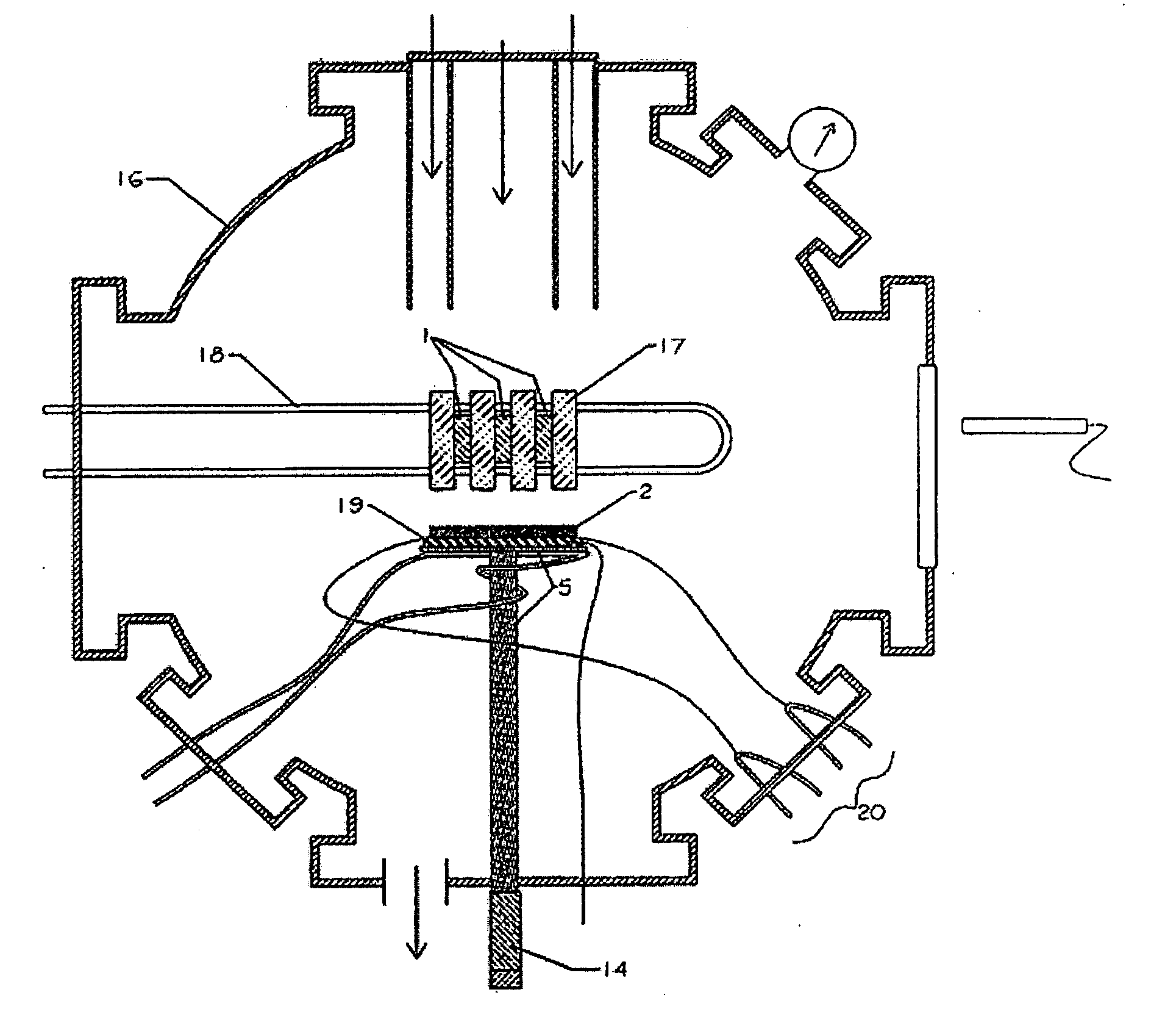
[0024]Embodiments also include an apparatus and method for growing large diameter single crystal high quality SiC for use in semiconductor, electrical device, jewelry manufacture and other purposes. Embodiments of the method may include the introduction of a seed crystal of a particular polytype upon a substrate heater. This substrate is then raised in temperature coincident with the raising of temperature of the filaments located above and in close proximity to the substrate. Upon achieving desired temperatures, the gas precursors may be flowed across the filaments thereby creating a chemical reaction which forms the desired compounds for forming silicon carbide. Following continuation of this process for the desired amount of time to achieve the desired crystal length across the entirety of the diameter, the apparatus may be stopped through a series of precise steps or continuous (e.g., analog) change to reduce or eliminate defects normally associated with cooling whereby the crystal is removed from the apparatus and processed into the desired size(s) and shape(s).

Problems solved by technology

Despite major development efforts over many years, several quality issues pertaining to the high temperatures required for boule formation remain.
Seeded sublimation techniques have several disadvantages: First, contamination from the graphite crucibles and source material lead to unacceptable impurity levels in the bulk crystals.
These impurities lead to high unintentional carrier concentrations in the material.
High resistivity wafers required for several applications remain extremely expensive.
Additionally, high levels of defects in the crystal remain a concern.
Inhomogeneous temperature distribution increases the probability of graphite inclusion or Si droplet formation, which can lead to micropipes and other defects Particles shedding from the graphite crucible have also been observed as a significant culprit for defects.
Finally, the geometries associated with this technique make it extremely difficult to produce large diameter boules due to nonuniform temperatures in the boule and source material as the diameter of the sublimation system increases.
Major advantages of this technique include polytype stability and low defect density, but the low solubility of carbon at reduced temperatures and the high silicon vapor pressure make this method difficult for growing silicon carbide boules.
Also, silicon is very reactive at high temperatures and no suitable crucible material has been found.
These factors have so far made LPE growth impractical: see D. H. Hofmann and M. H. Muller, “Prospects of the use of liquid phase techniques for the growth of bulk silicon carbide crystals”, Mat. Sci. and Eng.
Conversely in HTCVD the gas supply is essentially inexhaustible with the correct set-up, and the flowrates can be continuously tightly controlled, which makes the potential boule length only limited by the chamber design.
However, many of the same problems associated with evaporation techniques will occur with HTCVD, such as high levels of impurities in the SiC from the graphite walls, and stress on the crystal formed due to the high growth temperatures.
In addition, the reactions that occur at the walls of HTCVD reactors limit the diameter of uniform growth due to heat and mass transfer considerations.
Although thermal CVD can produce single crystal layers, growthrates of SiC tend to be too low for the economic production of boules.
The substrate temperature for these depositions are in sharp contrast to sublimation and HTCVD techniques, which require substrate temperatures in excess of 2000° C. The prior art shows that the HFCVD technique can produce monocrystalline SiC in layers that are relatively thin, but the systems used for the growth of thin layers are not designed to deposit for the length of time required to grow boules.
Also these systems will have contamination and growth time issues associated with the filaments at temperatures required to produce the growthrates needed for economic boule growth.
The advantages of SiC devices have yet to be extensively realized on a commercial level because of the technology for growing SiC boules used to produce substrates is relatively immature.
Despite years of optimization efforts, the sublimation techniques used to produce most commercial SiC wafers continue to be plagued by high contamination and defect levels.
Also, the adoption of SiC as a substrate material has been limited by the high cost and small diameters of the wafers currently available.

Method used


Image

  • Production of bulk silicon carbide with hot-filament chemical vapor deposition
  • Production of bulk silicon carbide with hot-filament chemical vapor deposition
  • Production of bulk silicon carbide with hot-filament chemical vapor deposition

Examples


Embodiment Construction

[0047]Methods and systems are described for the deposition of bulk silicon carbide (SiC) boules using hot-filament chemical vapor deposition (HFCVD).

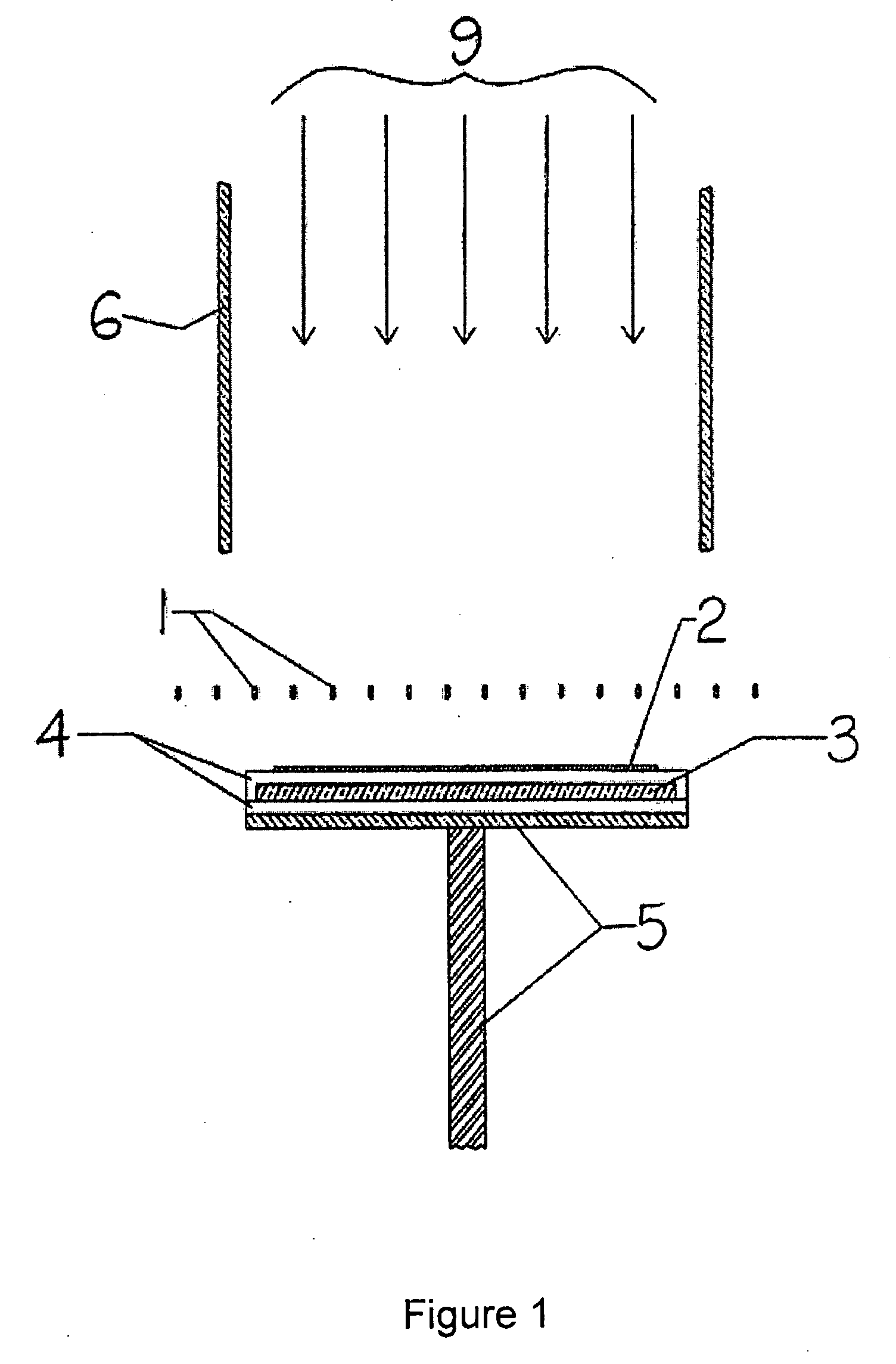
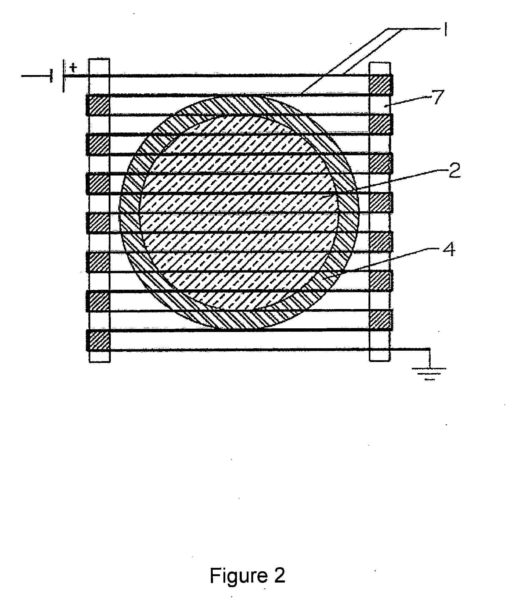
[0048]As depicted in FIG. 1, HFCVD techniques involve the passing of gas precursors 9 across heated filaments 1, where the precursors decompose into reactive intermediates which react with the heated substrate surface 2. Hot-filament chemical vapor deposition (HFCVD) allows the temperatures of the filaments and the substrate to be independently adjusted to permit the growth of large-scale SiC boules. Because the gas-phase temperature can be decoupled from the substrate, the substrate temperature can be reduced relative to sublimation, yielding materials with lower stress defects following a return to ambient temperature. The reduction in overall temperature variation from the chamber's deposition temperature to room temperature for additional processing can substantially reduce stress related defects in the boule. The ability to grow bo...


PUM

PropertyMeasurementUnit
diameteraaaaaaaaaa
thicknessaaaaaaaaaa
thicknessaaaaaaaaaa

Abstract

A method to grow a boule of silicon carbide is described. The method may include flowing a silicon-containing precursor and a carbon-containing precursor proximate to a heated filament array and forming the silicon carbide boule on a substrate from reactions of the heated silicon-containing and carbon-containing precursors. Also, an apparatus for growing a silicon carbide boule is described. The apparatus may include a deposition chamber to deposit silicon carbide on a substrate, and a precursor transport system for introducing silicon-containing and carbon-containing precursors into the deposition chamber. The apparatus may also include at least one filament or filament segment capable of being heated to a temperature that can activate the precursors, and a substrate pedestal to hold a deposition substrate upon which the silicon carbide boule is grown. The pedestal may be operable to change the distance between the substrate and the filament as the silicon carbide boule is grown.

Description

CROSS-REFERENCES TO RELATED APPLICATIONS[0001]This application claims the benefit of U.S. Provisional Application No. 60 / 954,789 to Robbins et al, filed Aug. 8, 2007, the entire contents of which are herein incorporated by reference for all purposes.STATEMENT AS TO RIGHTS TO INVENTIONS MADE UNDER FEDERALLY SPONSORED RESEARCH OR DEVELOPMENT[0002]This invention was developed at least partially with United States Government support under Grant No. 0637287 and Grant No. 0750064 from the National Science Foundation. The United States Government may have certain rights in this invention.FIELD OF INVENTION[0003]The present invention in general relates to the growth of silicon carbide boules. More specifically, the present invention relates to methods and apparatuses for growing silicon carbide boules using a hot-filament chemical vapor deposition system.BACKGROUND OF THE INVENTION[0004]Silicon carbide has superior properties regarding high-power, high-frequency, and high-temperature electr...

Claims


Application Information

Patent Timeline
Patent Type & Authority Applications(United States)
IPC IPC(8): C30B25/10
CPCC23C16/325C23C16/4583C30B29/36C30B25/00C23C16/52
Inventor ROBBINS, JOSHUASEMAN, MICHAEL
Owner BASIC 3C
Learn More