

Encapsulated silicidation for improved SiC processing and device yield
a technology of silic acid and silicide, applied in the field of silicide contact formation on a sic substrate, can solve the problems of reducing the contact resistance and possibly the reliability of the device, affecting the operation of the device, and causing stringers
- Summary
- Abstract
- Description
- Claims
- Application Information
AI Technical Summary
Benefits of technology
Problems solved by technology
Method used
Image

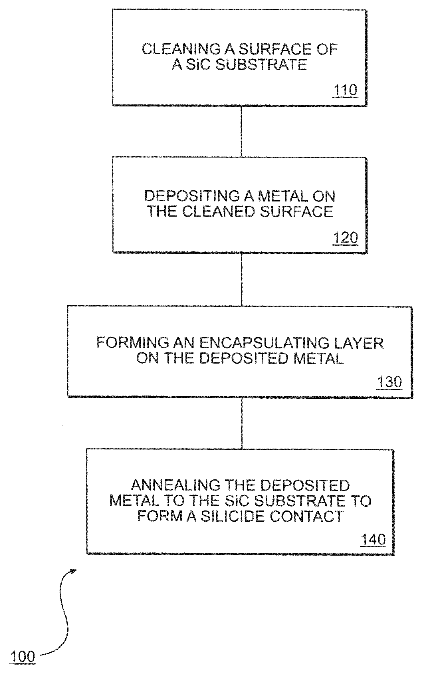
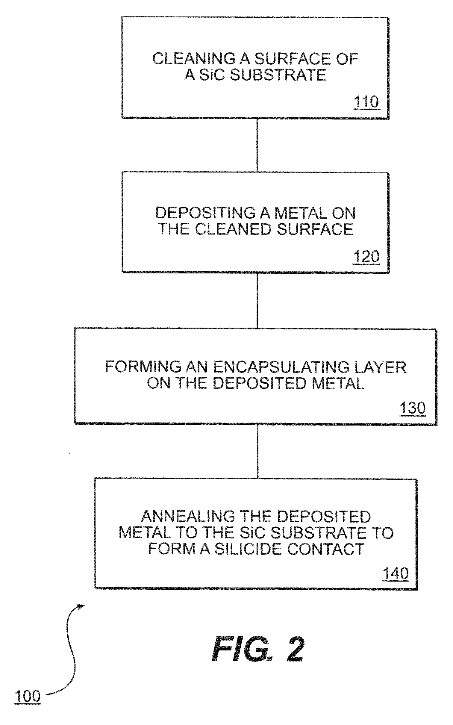
Examples
example 1
Encapsulating Nickel Deposit with a Titanium Layer Prevents Stringer Formation and Agglomeration During Nickel Suicide Formation
[0033]A SiC wafer was etched in 10% HF to remove any native oxide on the wafer surface. The etched SiC wafer was washed with isopropanol and dried with nitrogen gas and immediately loaded into the growth chamber of an e-beam evaporation device (e.g. CHA E-Beam Evaporation System (CHA Industries, Fremont, Calif.), pumped down to <1 μTorr). Nickel was deposited on the SiC using the standard e-beam deposition procedure setting the e-beam evaporator to a 10 A / minute deposition rate. A titanium layer was then also formed on the deposited nickel by e-beam deposition. The deposited layers then underwent rapid-thermal annealing in Ar at 900° C. for 30 seconds, and 980° C. for 60 seconds using an Axcelis Reliance 850 RTA system (Axcelis Technologies Inc., Beverly, Mass.).
[0034]Titanium was selected as the encapsulating layer because it adheres well to the nickel dep...
example 2
Molybdenum or Tetra-Ethoxy-Silane (TEOS) Deposited Oxide Layer on Nickel Deposit Suffered Cracking and / or Delamination During Silicidation Annealing Process
[0036]A SiC wafer was etched in 10% HF to remove any native oxide. The etched SiC wafer was washed with isopropanol and dried with nitrogen gas and immediately loaded into the growth chamber of an e-beam evaporation device (e.g. CHA E-Beam Evaporation System, pumped down to <1 μTorr). Nickel was deposited on the SiC using the standard e-beam deposition procedure, setting the e-beam evaporator to a 10 A / minute deposition rate. A molybdenum layer was then formed on the deposited nickel also by e-beam deposition. The deposited layers then under went rapid-thermal annealing in Ar at 900° C. for 30 seconds, and 980° C. for 60 seconds using an Axcelis Reliance 850 RTA system. As shown in FIG. 5, the molybdenum encapsulating layer was delaminated after the annealing process.
[0037]In another experiment, a TEOS silicon dioxide layer was d...
example 3
Devices Produced Using Titanium Encapsulated Nickel Silicide Contacts
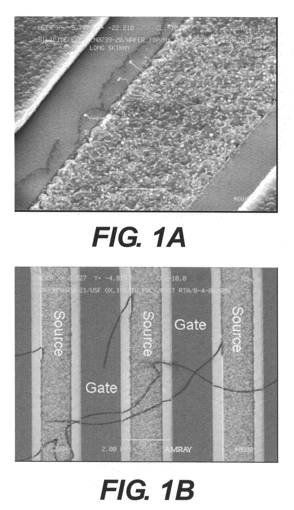
[0039]Several MOSFET devices were created using titanium encapsulated nickel silicide contacts. Besides the encapsulating step, the processes used to create the devices were all standard MOSFET fabrication processes well known to one skilled in the art. The processing of these MOSFETs used a planar double implantation DMOSFET vertical structure and process sequence typical of such high voltage SiC devices. FIG. 7 shows a picture of large area 10 kV SiC MOSFETs that use the titanium encapsulated nickel silicide contacts.
[0040]Electrical testing on the MOSFETs was performed using a micromanipulator probe set up with a Tektronix 371A High Power Curve Tracer for the forward (on) characteristics and a Trek Model 20 / 20C High Voltage Amplifier with the device immersed in flouinert to measure the reverse (OFF) characteristics.
[0041]FIG. 8 is a plot showing the IV characteristics of a large (1 cm2 chip area, 0.6 cm2 active)...
PUM
| Property | Measurement | Unit |
|---|---|---|
| temperature | aaaaa | aaaaa |
| thickness | aaaaa | aaaaa |
| thickness | aaaaa | aaaaa |
Abstract
Description
Claims
Application Information