

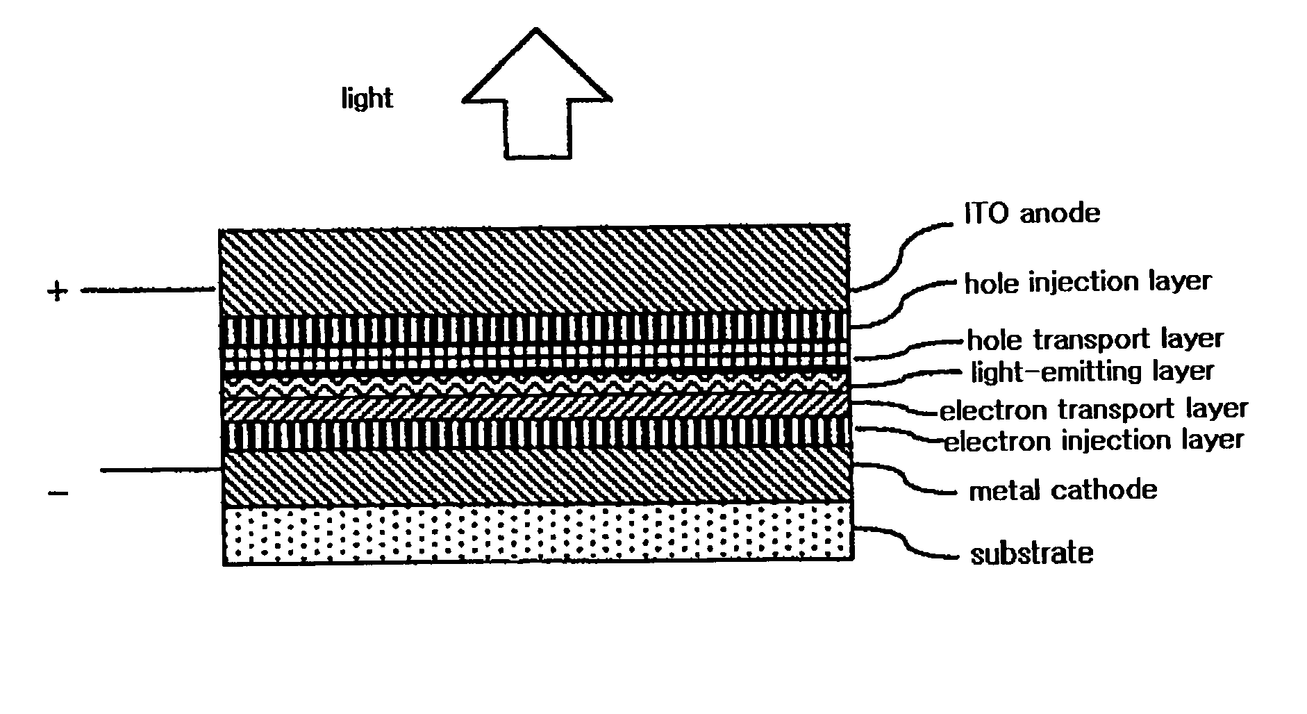
Organic light-emitting device comprising buffer layer and method for fabricating the same
a light-emitting device and buffer layer technology, applied in the direction of organic semiconductor devices, discharge tube luminescnet screens, organic chemistry, etc., can solve the problems of reducing the effective display aperture ratio, increasing the operating voltage of the organic light-emitting device, and increasing the operating voltage. , to achieve the effect of destroying the organic layer and forming an electrode on the organic layer
- Summary
- Abstract
- Description
- Claims
- Application Information
AI Technical Summary
Benefits of technology
Problems solved by technology
Method used
Image

Examples
examples 1-5
[0077] On a glass substrate, a cathode (Al) having a thickness of 150 nm and an electron injection layer (LiF) having a thickness of 1.5 nm were sequentially formed by a thermal evaporation process. Then, on the electron injection layer, an electron transport layer consisting of a thin film made of a material represented by the following formula 2-1 comprising imidazole group was formed to a thickness of 20 nm.
[0078] Then, on the electron transport layer, an Alq3 light-emitting host was co-deposited with C545T (10-(2-benzothiazolyl)-1,1,7,7-tetramethyl-2,3,6,7-tetrahyro-1H,5H,11H-1)benzopyrano[6,7,8-ij]quinolizin-11-one) to form a light-emitting layer having a thickness of 30 nm. On the light-emitting layer, a hole transport layer consisting of a thin film made of NPB (4,4′-bis[N-(1-napthyl)-N-phenylamino]biphenyl) was deposited to a thickness of 40 nm. On the hole transport layer, a hole injection / buffer layer made of a compound represented by the following formula 1-1 was formed...
example 6
[0080] A both-side emission type organic light-emitting device was fabricated in the same manner as described in Examples 1-5 except that a cathode consisting of an thin Al film having a very small thickness of 5 nm formed on an ITO film having a thickness of 150 nm is used in place of the cathode consisting of the thin Al film having a thickness of 150 nm.
[0081] [Measurement of Current-Voltage Characteristics and Light Emission Characteristics of Device]
[0082] To the organic light-emitting device fabricated in Example 1, each of reverse and forward electric fields was applied at a voltage increasing at increments of 0.2 volts while current at each voltage value was measured. The measurement results are shown in FIGS. 6 and 7, respectively. Also, to the organic light-emitting device fabricated in Example 1, current was applied while gradually increasing current density from 10 mA / cm2 to 100 mA / cm2, and at the same time, the luminous intensity of the device was measured using photom...
example 7
[0087] On a glass substrate, a cathode (Al) having a thickness of 150 nm and an electron injection layer (LiF) having a thickness of 1.5 nm were sequentially formed by a thermal evaporation process. Then, on the electron injection layer, an electron transport layer consisting of a thin film made of the material comprising imidazole group represented by the above formula 2-1 was formed to a thickness of 150 nm. On the electron transport layer, an electron injection layer (LiF) having a thickness of 1.5 nm and Al layer having a thickness of 150 nm were formed sequentially to fabricate a symmetrical-type device as shown in FIG. 13 in which electric current runs only through electrons.
PUM
 Abstract
Description
Claims
Application Information