

High speed electronics interconnect and method of manufacture
a high-speed electronics and interconnecting technology, applied in the direction of waveguides, high-frequency circuit adaptations, waveguide type devices, etc., can solve the problems of increasing the number of on-chip interconnections, increasing the difficulty of interconnecting electronic devices without sacrificing signal speed, and increasing the density of interconnections, so as to reduce the effective dielectric constant and reduce the effective dielectric loss , the effect of increasing the bandwidth of on-chip and off-chip interconnections
- Summary
- Abstract
- Description
- Claims
- Application Information
AI Technical Summary
Benefits of technology
Problems solved by technology
Method used
Image

Examples
first embodiment
[0080]An important aspect of a high speed electronic interconnection is that the microwave loss is reduced by reducing the effective dielectric constant, resulting in increased bandwidth of the interconnection, thereby reaching a signal speed in the interconnection that approaches closer to the source signal speed. According to a second important aspect of the invention, the technique is cost effective and compatible with standard manufacturing technologies known in the art.
[0081]In an on-chip interconnection between two or more interconnected electronic elements (such as transistors, ICs, etc.), an electrical signal at a low speed can be communicated through an electrical signal conductor in form of a wire laid on a dielectric medium. However, for communicating an electrical signal at a high-speed, an electrical signal conductor must be a microstrip line type, or a strip line type transmission line.
[0082]In the following sections, preferred embodiments of the invention will be dis...
second embodiment
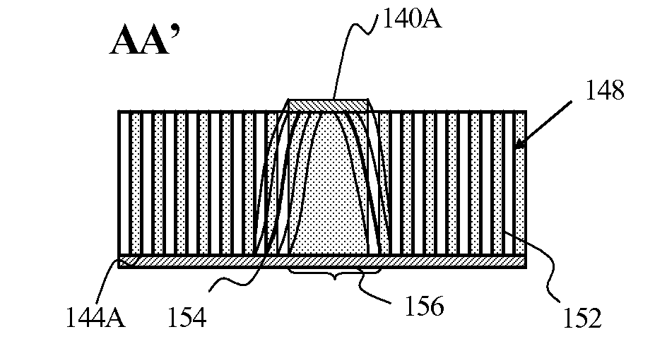
[0086]FIGS. 10A, 10B, 10C, and 10D collectively represent the invention, wherein to avoid repeated explanation, like parts are indicated by like reference numerals as used in FIGS. 8A-8C. More specifically, FIG. 10A is a top view of an interconnection and FIGS. 10B, 10C, and 10D are the enlarged cross-sectional views of an interconnection system along the line AA′ shown in FIG. 10A. In FIGS. 10A, 10B, 10C, and 10D, the microstrip line type of transmission line consisting of signal lines 140C, 140D, and 140E and back-side ground lines 144C, 144D, and 144E, laid on to a periodic dielectric structure 168 consisting of dielectric spheres or cylinders 150, with diameter 2r (FIG. 10D) and span a (FIG. 10A), similar to the periodic dielectric array described earlier in reference with FIGS. 8A-C, and a backside slot 164. According to principles of the invention, the effective dielectric constant (i.e. microwave index) is substantially reduced, and the electrical field intensity 170 (FIG. 10...
eighth embodiment
[0103]FIG. 17 shows a flow-chart of a printed circuit board (PCB) fabrication process for an off-chip interconnections system in an eighth embodiment in accordance with the principles of the invention, wherein like parts are indicated by like numerals, so that repeated explanation is omitted here. A dielectric sheet (not shown) is made using a standard PCB technology, for example a slurry casting process in which the slurry is cast into about 200 μm to 500 μm thick ceramic sheets by a slip cast process. To make the preorder dielectric structure 244, arrays of air holes are made into the dielectric substrate using processes such as laser drilling, dry-etching, or wet-etching (following patterning for etching). Via holes are formed through the dielectric sheet with air holes 244 by a punching machine with punches and dies. For example, ceramic sheet 244 may have more than 10,000 via holes in a 250 mm square area. A low resistivity conductor paste is applied onto the punch sheet. In th...
PUM
| Property | Measurement | Unit |
|---|---|---|
| Dielectric polarization enthalpy | aaaaa | aaaaa |
| Diameter | aaaaa | aaaaa |
| Dielectric constant | aaaaa | aaaaa |
Abstract
Description
Claims
Application Information