Semiconductor device and method for manufacturing the same

a semiconductor and semiconductor technology, applied in the direction of semiconductor devices, electrical devices, transistors, etc., can solve the problems of deterioration of capacitor characteristics, glass substrate cannot be subjected to heat treatment, and it is difficult to perform high heat treatment on the dielectric layer of the capacitor element, so as to reduce the area, reduce the area, and increase the relative permittivity

Inactive Publication Date: 2009-04-02
SEMICON ENERGY LAB CO LTD
View PDF8 Cites 8 Cited by
  • Summary
  • Abstract
  • Description
  • Claims
  • Application Information

AI Technical Summary

Benefits of technology

[0016]When a capacitor portion is provided with a dielectric layer that contains a material with a relative permittivity of 10 or more, for example, yttrium oxide or a mixture of yttrium oxide and zirconium oxide, the capacitor portion in an integrated circuit can be reduced in area.
[0017]Before a crystalline silicon layer separated from a single crystal silicon substrate is bonded to a supporting substrate, a YSZ film as a high dielectric film is formed over the single crystal silicon substrate and heat treatment is performed, thereby obtaining a semiconductor device with a higher relative permittivity in which a capacitor portion in an integrated circuit is reduced in area. In particular, a desired semiconductor device can be manufactured by the aforementioned method even over a supporting substrate with an upper temperature limit of less than 750° C. that is a heat treatment temperature effective for a YSZ film. In addition, the circuit design can be made without reducing the thickness of the insulating film in the storage capacitor portion; therefore, the storage capacitor portion having excellent charge retention characteristics can be obtained.

Problems solved by technology

However, the leakage current increases with reduction in thickness of the dielectric layer, leading to deterioration of characteristics of the capacitor element.
A glass substrate cannot be subjected to heat treatment at a high temperature of about 700° C. or higher; therefore, it is difficult to perform high heat treatment on a dielectric layer of a capacitor element, which has been deposited over a glass substrate.

Method used


Image

  • Semiconductor device and method for manufacturing the same
  • Semiconductor device and method for manufacturing the same
  • Semiconductor device and method for manufacturing the same

Examples


embodiment mode 1

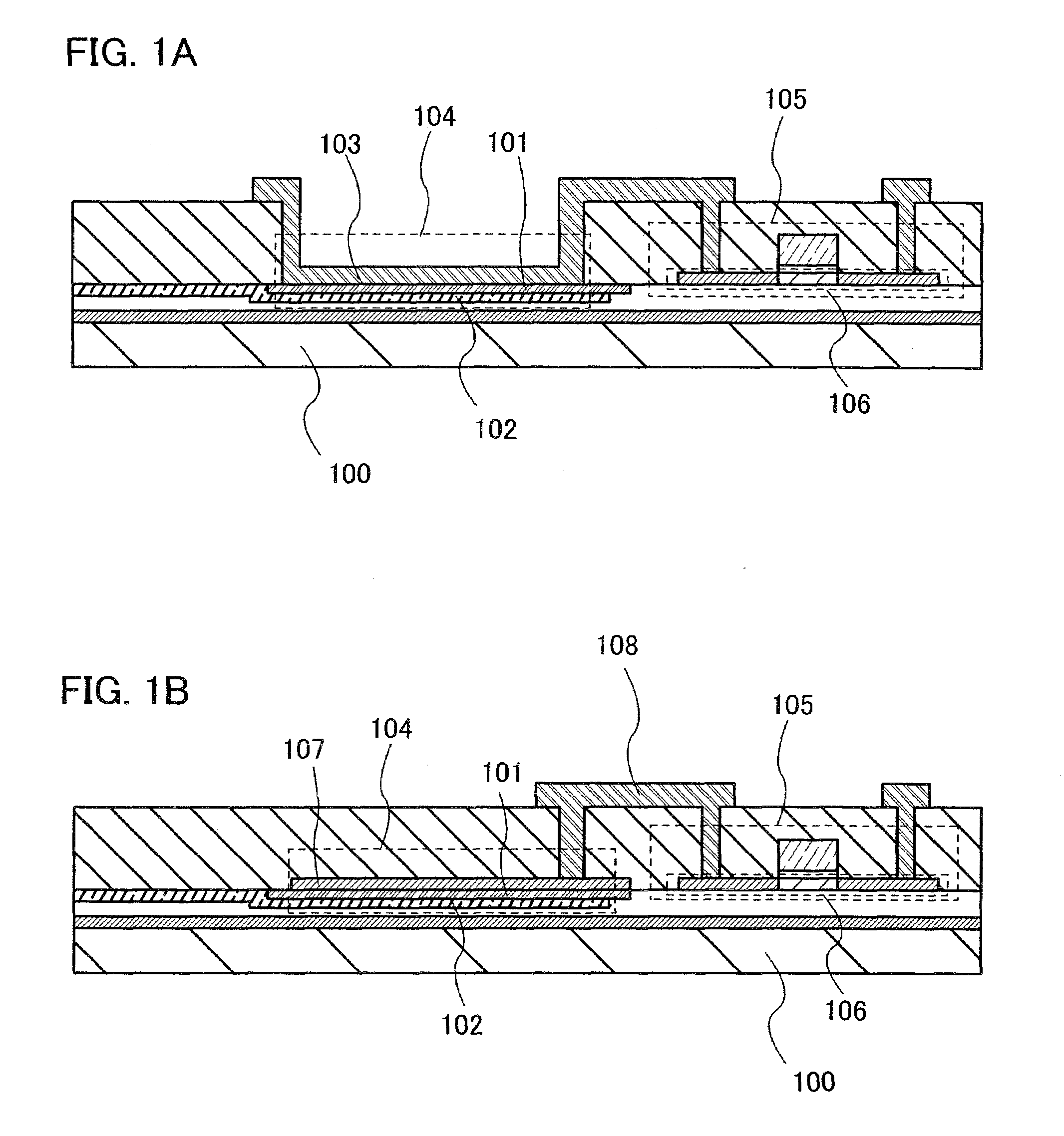
[0028]A structure of a semiconductor device according to the invention is described with reference to FIGS. 1A and 1B.

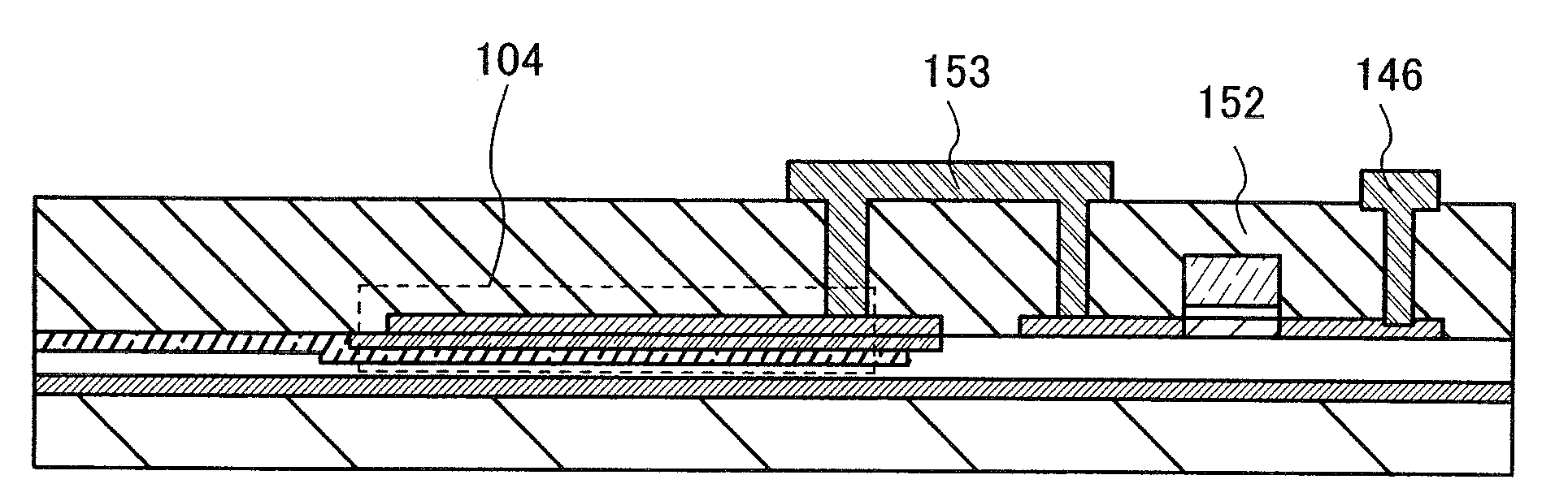
[0029]In FIG. 1A, a storage capacitor portion insulating layer 101 containing yttrium oxide or YSZ, a storage capacitor portion lower electrode 102, and a wiring 103 are formed over a supporting substrate 100. The wiring 103 also serves as a storage capacitor portion upper electrode. A storage capacitor portion 104 is formed at a position where a portion in which the storage capacitor portion lower electrode 102 is in contact with the storage capacitor portion insulating layer 101 overlaps a portion in which the storage capacitor portion insulating layer 101 is in contact with the wiring 103 as viewed from the top of the supporting substrate. A TFT 105 is formed over the same supporting substrate 100. The TFT 105 includes an active layer 106 that is a crystalline silicon layer. That is to say, the portion in which the storage capacitor portion lower electrode 102 is ...

embodiment mode 2

[0091]In this embodiment mode, a semiconductor device including an SOI substrate and a TFT is described with reference to FIGS. 7 and 8.

[0092]FIG. 7 illustrates a microprocessor 200 as an example of a semiconductor device. The microprocessor 200 includes an arithmetic logic unit (ALU) 201, an ALU controller 202, an instruction decoder 203, an interrupt controller 204, a timing controller 205, a register 206, a register controller 207, a bus interface (Bus I / F) 208, a read only memory (ROM) 209, and a ROM interface (ROM I / F) 210.

[0093]An instruction input to the microprocessor 200 through the bus interface 208 is input to the instruction decoder 203, decoded therein, and then input to the ALU controller 202, the interrupt controller 204, the register controller 207, and the timing controller 205. The ALU controller 202, the interrupt controller 204, the register controller 207, and the timing controller 205 conduct various controls based on the decoded instruction. Specifically, the ...


PUM


Abstract

A method for manufacturing a semiconductor device with high response speed and high reliability. In the method for manufacturing a semiconductor device of the invention, a bonding layer is formed over a substrate, an insulating film and a storage capacitor portion lower electrode are formed over the bonding layer, a single crystal silicon layer is formed over the insulating film, a storage capacitor portion insulating film is formed over the storage capacitor portion lower electrode, a wiring is formed over the storage capacitor portion insulating film, a channel forming region and a low concentration impurity region are formed over the single crystal silicon layer, and a gate insulating film and a gate electrode are formed over the single crystal silicon layer. The storage capacitor portion insulating film is formed by depositing a YSZ film with a single crystal silicon layer used as a base film, whereby the permittivity increases and thus the leakage current from the storage capacitor portion is suppressed.

Description

BACKGROUND OF THE INVENTION[0001]1. Field of the Invention[0002]The present invention relates to a semiconductor device and a method for manufacturing the same. In particular, the invention relates to a substrate having an SOI (silicon on insulator) structure in which a semiconductor layer is formed by slicing a crystalline semiconductor substrate and bonded to a different kind of substrate. More particularly, the invention relates to a bonding SOI technique and a method for manufacturing an SOI substrate in which a single crystal or polycrystalline semiconductor layer is bonded to a substrate having an insulating surface such as a glass substrate. Furthermore, the invention relates to a display device or a semiconductor device having such an SOI structure.[0003]2. Description of the Related Art[0004]Instead of silicon wafers manufactured by slicing a single crystal semiconductor ingot, semiconductor substrates called silicon on insulators (SOI substrates) in which a thin single cry...

Claims


Application Information

Patent Timeline
Patent Type & Authority Applications(United States)
IPC IPC(8): H01L21/8242H01L27/12
CPCH01L27/1266H01L27/1255H01L29/78654H01L29/04
Inventor AKIMOTO, KENGO
Owner SEMICON ENERGY LAB CO LTD
Why Eureka
Try Eureka