Radiation-Sensitive, Wet Developable Bottom Antireflective Coating Compositions and Their Applications in Semiconductor Manufacturing

a technology of anti-reflective coatings and compositions, applied in the direction of photosensitive materials, instruments, photomechanical treatment, etc., can solve the problems of line width variation, thin film interference (or standing waves), and reflective notching, so as to reduce or eliminate scumming and minimize or prevent undercutting

Inactive Publication Date: 2009-04-16
JSR MICRO
View PDF25 Cites 28 Cited by
  • Summary
  • Abstract
  • Description
  • Claims
  • Application Information

AI Technical Summary

Benefits of technology

[0011]The present invention is directed to compositions for forming photosensitive, wet developable bottom antireflective coatings (DBARCs) and their applications in high-resolution, photolithographic semiconductor manufacturing. Among other inventive features, the invention reduces or eliminates scumming by utilizing a photoacid generator (PAG) that produces a sufficiently acidic photoacid upon exposure to activating radiation. Further, the invention minimizes or prevents undercutting by using a photoacid that is not too acidic and by controlling the rate and extent of anisotropic photoacid diffusion through the DBARC and photoresist. The invention controls the photoacid diffusion by using a photoacid of a certain minimum size and by controlling the temperature of a post-exposure baking step in the photolithographic process.

Problems solved by technology

Back reflectivity can cause thin film interference (or standing waves) and reflective notching.
Thin film interference results in changes in critical line width dimensions caused by variations in the total light intensity in the photoresist film as the thickness of the photoresist changes.
Reflective notching becomes severe as the photoresist is patterned over substrates containing topographical features, which scatter light through the photoresist film, leading to line width variations and, in extreme cases, forming regions with complete photoresist loss.
At shorter wavelengths, reflection from the substrate becomes increasingly detrimental to the lithographic performance of the photoresist.
The BARC remains behind post-development due to the crosslinked nature of the BARC, which leads to the need for an etch step.
Neither of these approaches, however, is as effective as a BARC with respect to reflectivity control and, ultimately, critical dimension control.
Presently, trench scumming and line undercut pose an obstacle to the adoption of DBARCs in high-volume semiconductor manufacturing of critical device features of a size ≦130 nm.
In the wet development process with conventional DBARC systems, the DBARC is removed vertically at the same rate as horizontally, leading to undercutting of the photoresist lines.
Such undercutting can result in line lifting and line collapse at smaller (<200 nm) sizes of photoresist lines.

Method used


Image

  • Radiation-Sensitive, Wet Developable Bottom Antireflective Coating Compositions and Their Applications in Semiconductor Manufacturing
  • Radiation-Sensitive, Wet Developable Bottom Antireflective Coating Compositions and Their Applications in Semiconductor Manufacturing
  • Radiation-Sensitive, Wet Developable Bottom Antireflective Coating Compositions and Their Applications in Semiconductor Manufacturing

Examples


example 1

Calculation of Molar Volume of Photoacids

[0236]The molar volume of various photoacids was calculated using the ACD ChemSketch 10.0 program available from Advance Chemistry Development, Inc. Chemical structures were drawn and the size of the photoacids was calculated in terms of molar volume. The molar volume of representative photogenerated acids, reported in units of cm3, is shown in Table 1.

TABLE 1Molar volume of photoacidsPhotoacidMolar Volume (±3 cm3)(CF3SO2)3CH207.2(CF3SO2)2NH145.2(CF3CF2SO2)2NH200.1[CF3(CF2)3SO2]2NH309.9

example 2

Photolithography Using Novel DBARC Composition I and Resist I

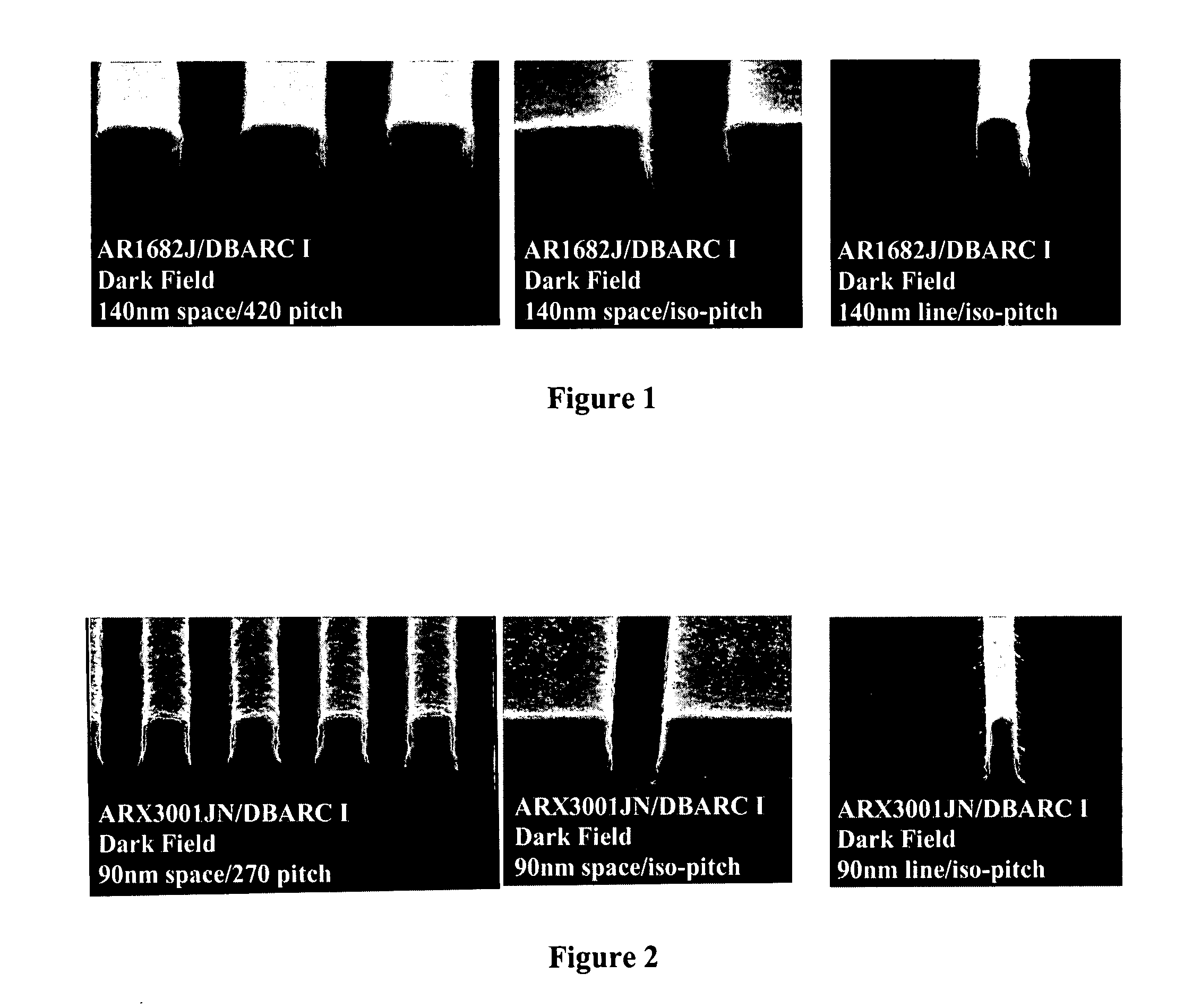
[0237]To 10 ml of DBARC solution BSI.W06055B 07193.001JL (available from Brewer Science Inc., Rolla, Mo.) containing 0.1175 g of polymer and 0.0425 g of crosslinker and dye were added 2.065 mg of triphenylsulfonium tris(trifluoromethanesulfonyl)methide and 0.245 mg of 1-piperidine ethanol as quencher. The resulting DBARC solution was filtered through a 0.5 micron filter. A silicon wafer was coated with 550 Å of the DBARC solution prepared above and hard-baked at 160° C. for 60 seconds. Next, the DBARC-coated wafer was coated with 1950 Å of JSR ARX1682J photoresist (available from JSR Micro, San Jose, Calif.) and soft-baked at 110° C. for 60 seconds. The coated wafer was then exposed to 193 nm UV radiation through a binary chrome-on-glass mask using Nikon S305B scanner. After exposure the wafer was baked at 110° C. for 60 sec. and wet developed for 40 sec. using PD523 trimethylammonium hydroxide developer (available from Mo...

example 3

Photolithography Using Novel DBARC Composition I and Resist II

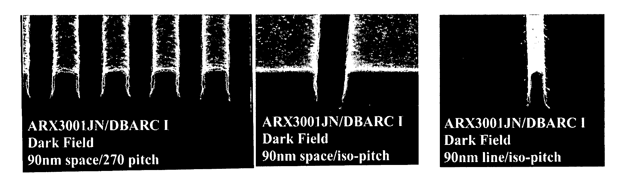
[0239]To 10 ml of DBARC solution BSI.W06055B 07193.001JL (available from Brewer Science) containing 0.1175 g of polymer and 0.0425 g of crosslinker and dye were added 2.065 mg of triphenylsulfonium tris(trifluoromethanesulfonyl)methide and 0.245 mg of 1-piperidine ethanol as quencher. The resulting DBARC solution was filtered through a 0.5 micron filter. A silicon wafer was coated with 550 Å of the DBARC solution prepared above and hard-baked at 160° C. for 60 sec. Next the DBARC-coated wafer was coated with 1950 Å of JSR ARX3001JN photoresist (available from JSR Micro) and soft-baked at 110° C. for 60 sec. The coated wafer was then exposed to 193 nm UV radiation through a binary chrome-on-glass mask using Nikon S3057E scanner. After exposure the wafer was then baked at 110° C. for 60 sec. and wet developed for 40 sec. using PD523 developer from Mosses Lake Industries. Finally the patterns formed on the wafer were analyze...


PUM

PropertyMeasurementUnit
temperatureaaaaaaaaaa
molar volumeaaaaaaaaaa

Abstract

The present invention is directed to novel radiation-sensitive, wet developable bottom antireflective coating (DBARC) compositions and their use in semiconductor device manufacturing. The DBARC compositions contain a photoacid generator that produces a photoacid upon exposure to activating radiation. In a photolithographic imaging process, the relatively strong photoacid reduces or eliminates scumming. Further, the relatively large size of the photoacid limits its diffusion through the DBARC, thus minimizing or preventing undercut. The inventive method also limits diffusion of the photoacid by controlling the temperature of the post-exposure baking step. Use of the DBARC compositions with a photoresist in photolithography results in highly resolved features having essentially vertical profiles and no scumming and no undercut, which is critical as microelectronics and semiconductor components become increasingly miniaturized.

Description

BACKGROUND[0001]1. Field of the Invention[0002]The present invention is directed to compositions for forming radiation-sensitive, wet developable bottom antireflective coatings and their use in photolithographic semiconductor manufacturing.[0003]2. Description of the State of the Art[0004]The power and capabilities of computers and microelectronic devices have increased dramatically over the years as a result of semiconductor manufacturers' ability to place ever more transistors and other critical components on microsubstrates (e.g., integrated circuits). With the increasing miniaturization of electronics components, high-resolution photolithography requires better materials and technology.[0005]Bottom antireflective coatings (BARCs) are used in semiconductor device manufacturing to reduce back reflection of light from reflective substrates. Back reflectivity can cause thin film interference (or standing waves) and reflective notching. Thin film interference results in changes in cr...

Claims


Application Information

Patent Timeline
Patent Type & Authority Applications(United States)
IPC IPC(8): G03C5/56
CPCG03F7/0045G03F7/0046G03F7/095G03F7/091G03F7/0392
Inventor PHAM, VICTORAYOTHI, RAMAKRISHNANSLEZAK, MARK
Owner JSR MICRO
Why Eureka
Try Eureka