Method for manufacturing semiconductor substrate and method for manufacturing semiconductor device

Inactive Publication Date: 2009-04-16
SEMICON ENERGY LAB CO LTD
View PDF25 Cites 53 Cited by
  • Summary
  • Abstract
  • Description
  • Claims
  • Application Information

AI Technical Summary

Benefits of technology

[0090]By a method for manufacturing a semiconductor substrate of the present invention, re-single-crystallization of a single crystal semiconductor layer which is separated from a single crystal semiconductor substrate can be performed at a process temperature of 700° C. or lower. In addition, the single crystal semiconductor layer which is separated from the single crystal semiconductor substrate

Problems solved by technology

However, a glass substrate has a strain point of 700° C. or lower and thus has low heat resistance.
Therefore, a glass substrate cannot be heated at a temperature which exceeds its upper temperature limit, and the process temperature is limited to be 700° C. or lower.
That is, there are also limitations on process temperature for a step of removing a crystal defect at a separation plane and a step of planarizing a surface.
Removal of a crystal defect in a semiconductor layer that has been attached to a silicon wafer has been conventionally achieved by heating at a temperature of 1000° C. or higher; however, such a high temperature process cannot be utilized for removal of a crystal defect in a semiconductor layer that is attached to a glass substrate having a strain point of 700° C. or lower.
That is, a re-single-crystallization method has not been established, by which a single crystal semiconductor layer that is attached to a glass substrate having a strain point of 700° C. or lower is recovered to a single crystal semiconductor layer hav

Method used


Image

  • Method for manufacturing semiconductor substrate and method for manufacturing semiconductor device
  • Method for manufacturing semiconductor substrate and method for manufacturing semiconductor device
  • Method for manufacturing semiconductor substrate and method for manufacturing semiconductor device

Examples


embodiment mode 1

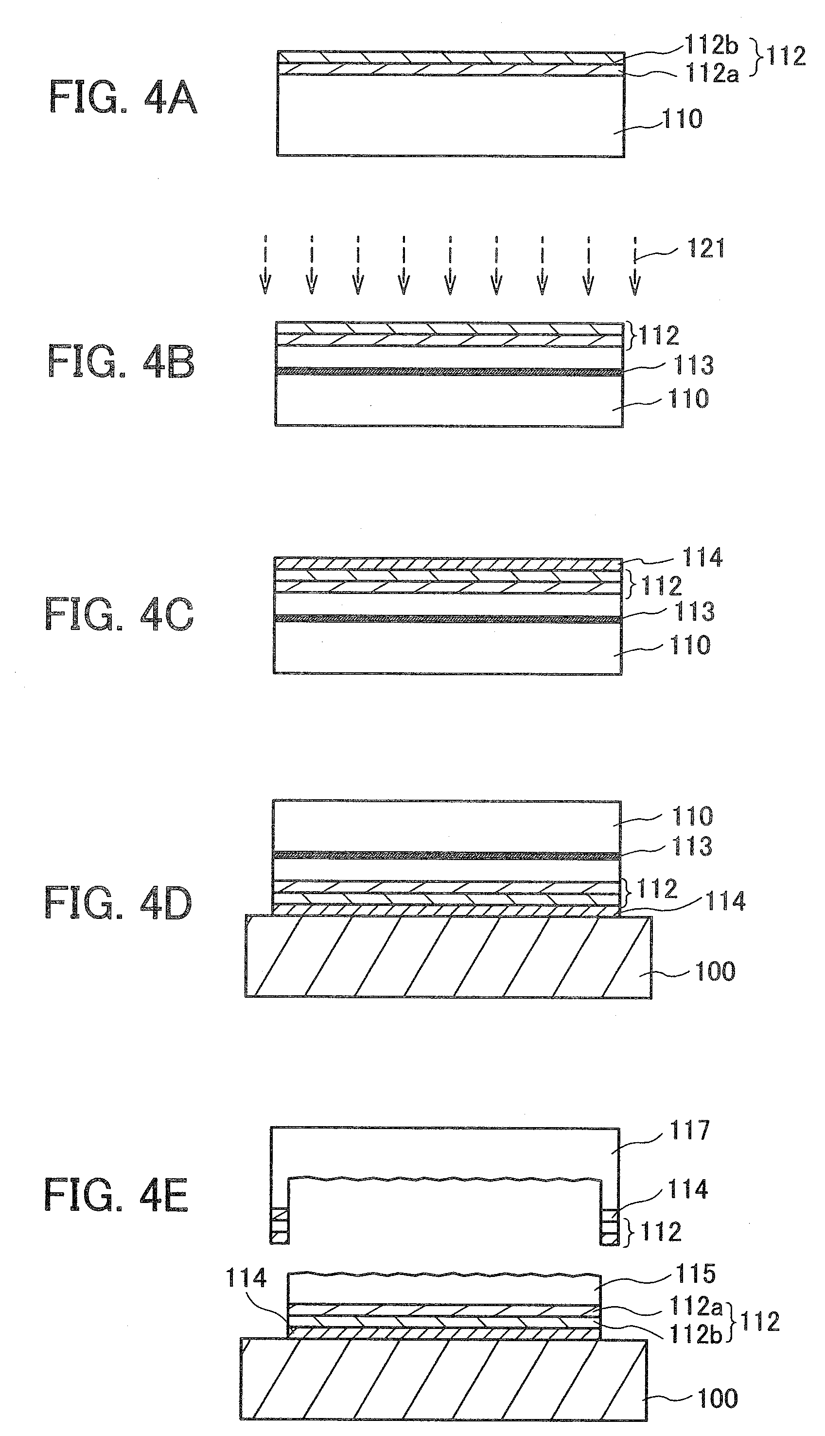
[0129]In this embodiment mode, a semiconductor substrate in which a single crystal semiconductor layer is fixed to a supporting substrate with a buffer layer interposed therebetween and a manufacturing method thereof will be described.

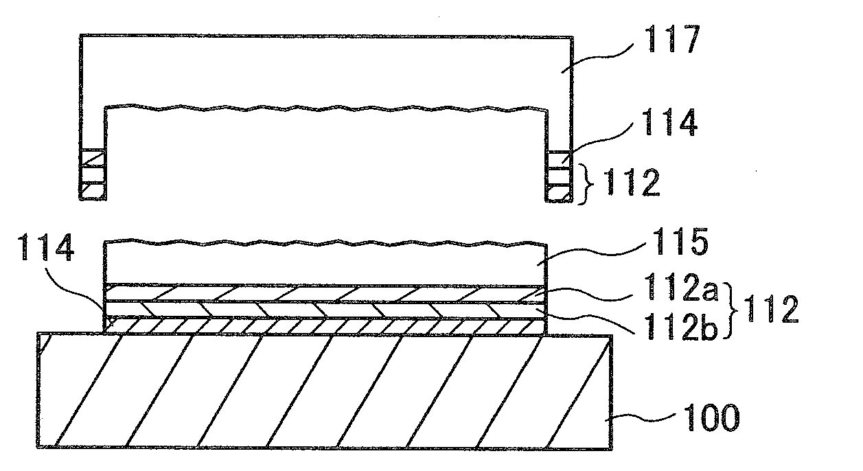
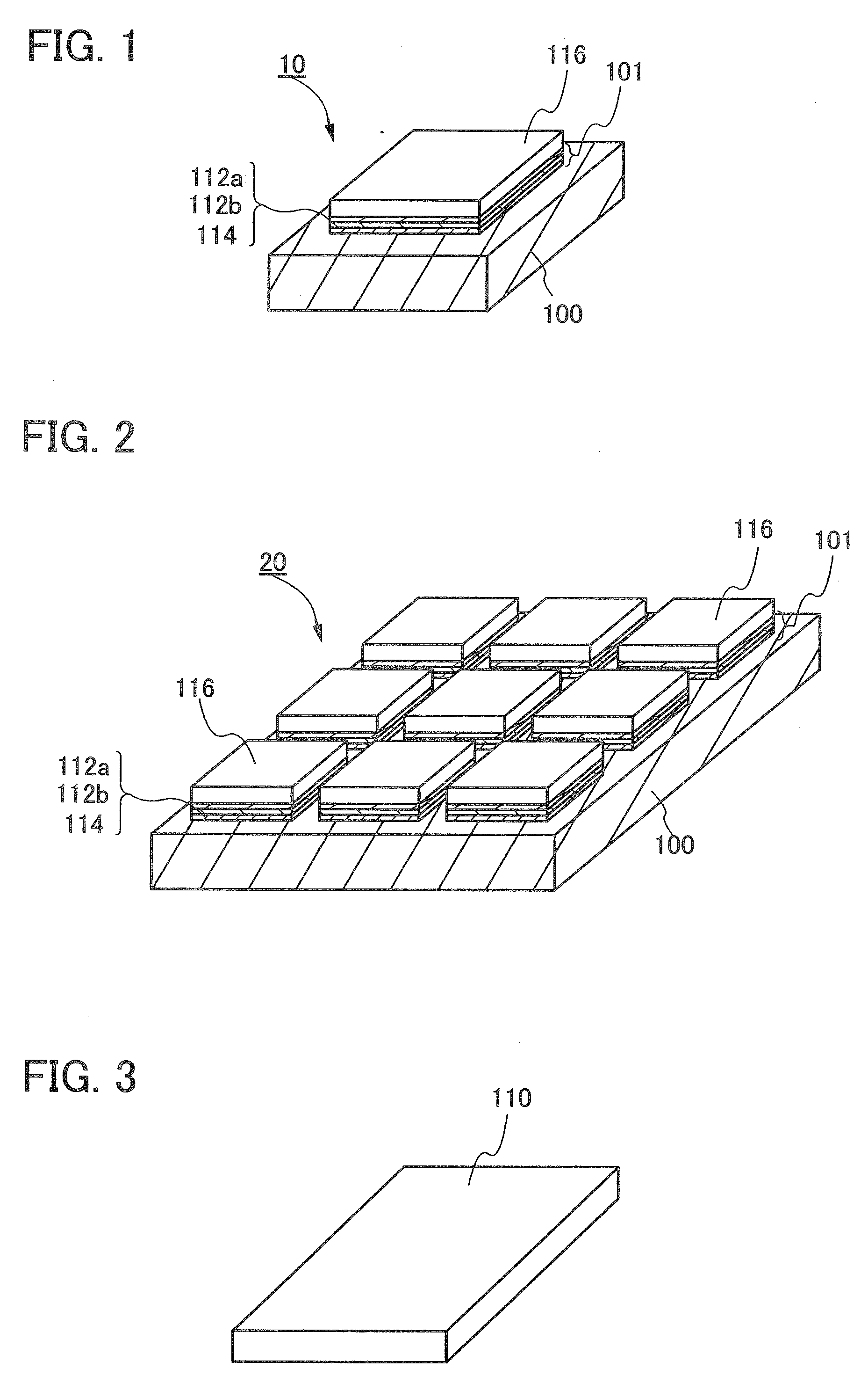
[0130]FIG. 1 is a perspective diagram which shows a structural example of a semiconductor substrate. In a semiconductor substrate 10, a single crystal semiconductor layer 116 is attached to the supporting substrate 100. The single crystal semiconductor layer 116 is provided over the supporting substrate 100 with a buffer layer 101 interposed therebetween. The semiconductor substrate 10 is a substrate having a so-called SOI structure, in which a single crystal semiconductor layer is formed over an insulating layer.

[0131]The buffer layer 101 may have a single-layer structure or a multilayer structure in which two or more layers are stacked. In this embodiment mode, the buffer layer 101 has a three-layer structure in which a bonding layer 114, an insulati...

embodiment mode 2

[0243]In this embodiment mode, a laser irradiation apparatus which can be used in an irradiation step of the laser beam 122 of FIG. 5A is described.

[0244]The laser irradiation apparatus of this embodiment mode has a laser, an optical system through which a laser beam generated by the laser passes, a stage for arranging an object, a gas ejection portion that is arranged between the optical system and the stage and ejects a nitrogen gas, a gas supply apparatus for supplying a gas to the gas ejection portion, and a gas heating apparatus for heating a nitrogen gas supplied from the gas supply apparatus.

[0245]The gas ejection portion includes an opening where a nitrogen gas is sprayed, a window through which a laser beam passes, and a frame provided with a cavity to which a nitrogen gas passed through a gas heating means is supplied. The gas heating means includes a heating element formed of ceramic.

[0246]A laser beam with which an object on the stage is irradiated passes through the opt...

embodiment mode 3

[0270]As an example of a manufacturing method of a semiconductor device using the semiconductor substrate 10, a manufacturing method of thin film transistors (TFTs) will be described in this embodiment mode, with reference to cross-sectional views of FIGS. 12A to 12D, FIGS. 13A to 13C, and FIG. 14. By combining a plurality of thin film transistors, a variety of types of semiconductor devices are manufactured. In this embodiment mode, an n-channel TFT and a p-channel TFT can be manufactured at the same time.

[0271]As illustrated in FIG. 12A, the single crystal semiconductor layer 116 over the supporting substrate 100 is processed (patterned) into a desired shape by etching, so that a semiconductor film 603 and a semiconductor film 604 are formed. A p-channel transistor is formed using the semiconductor film 603, and an n-channel transistor is formed using the semiconductor film 604.

[0272]To control threshold voltages, a p-type impurity element such as boron, aluminum, or gallium or an...


PUM


Abstract

An SOI substrate having a single crystal semiconductor layer with high surface planarity is manufactured. A semiconductor substrate is doped with hydrogen, whereby a damaged region which contains large quantity of hydrogen is formed. After a single crystal semiconductor substrate and a supporting substrate are bonded together, the semiconductor substrate is heated, whereby the single crystal semiconductor substrate is separated in the damaged region. While a heated high-purity nitrogen gas is sprayed on a separation plane of the single crystal semiconductor layer separated from the single crystal semiconductor substrate, laser beam irradiation is performed. By irradiation with a laser beam, the single crystal semiconductor layer is melted, whereby planarity of the surface of the single crystal semiconductor layer is improved and re-single-crystallization is performed.

Description

BACKGROUND OF THE INVENTION[0001]1. Field of the Invention[0002]The present invention relates to a method for manufacturing a semiconductor substrate having a semiconductor layer formed over an insulating layer and a method for manufacturing a semiconductor device.[0003]2. Description of the Related Art[0004]In recent years, integrated circuits using a silicon-on-insulator (SOI) substrate instead of a bulk silicon wafer have been developed. A feature of a thin single crystal silicon layer formed over an insulating layer can be taken advantage of to form a completely electrically separated semiconductor layer of a transistor in an integrated circuit and to form a completely depleted transistor. Accordingly, a semiconductor integrated circuit having high added values such as high integration, high-speed driving, and low power consumption can be realized.[0005]Known examples of SOI substrates are SIMOX substrates and bonded substrates. For example, an SOI structure of a SIMOX substrate...

Claims


Application Information

Patent Timeline
IPC IPC(8): H01L21/762H01L21/263
CPCH01L21/268H01L21/76254H01L29/78621H01L27/1266H01L27/1214H01L27/1218H01L27/1274H01L27/12
Inventor YAMAZAKI, SHUNPEI
Owner SEMICON ENERGY LAB CO LTD
Why Eureka
Try Eureka