Scalable high-k dielectric gate stack

a dielectric gate and high-k technology, applied in the field of semiconductor devices, can solve the problems of limiting the performance of conventional semiconductor oxide based gate electrodes, and the increase of the eot of the high-k gate dielectric stack by layers

Inactive Publication Date: 2009-04-30
SONY CORP +2
View PDF18 Cites 64 Cited by
  • Summary
  • Abstract
  • Description
  • Claims
  • Application Information

AI Technical Summary

Benefits of technology

[0080]oxidizing the second mixed high-k material layer, while preven

Problems solved by technology

High gate leakage current of silicon oxide and nitrided silicon dioxide as well as depletion effect of polysilicon gate electrodes limits the performance of conventional semiconductor oxide based gate electrodes.
An a

Method used


Image

  • Scalable high-k dielectric gate stack
  • Scalable high-k dielectric gate stack
  • Scalable high-k dielectric gate stack

Examples


first embodiment

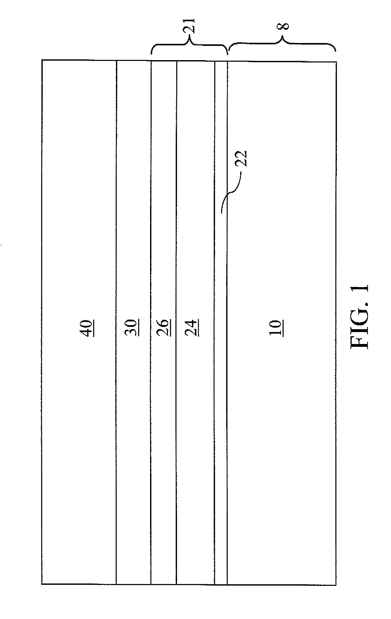
[0091]Referring to FIG. 1, a first exemplary semiconductor structure according to the present invention comprises a semiconductor substrate 8 containing a semiconductor region 10 comprising a semiconductor material, which may be selected from, but is not limited to, silicon, germanium, silicon-germanium alloy, silicon carbon alloy, silicon-germanium-carbon alloy, gallium arsenide, indium arsenide, indium phosphide, III-V compound semiconductor materials, II-VI compound semiconductor materials, organic semiconductor materials, and other compound semiconductor materials. Preferably, the semiconductor region 10 is single crystalline, i.e., have the same set of crystallographic orientations, or “epitaxial.”

[0092]The semiconductor substrate 8 may be a bulk substrate, a semiconductor-on-insulator (SOI) substrate, or a hybrid substrate having a bulk portion and an SOI portion. While the first embodiment is described with a bulk substrate, embodiments employing an SOI substrate or a hybrid ...

second embodiment

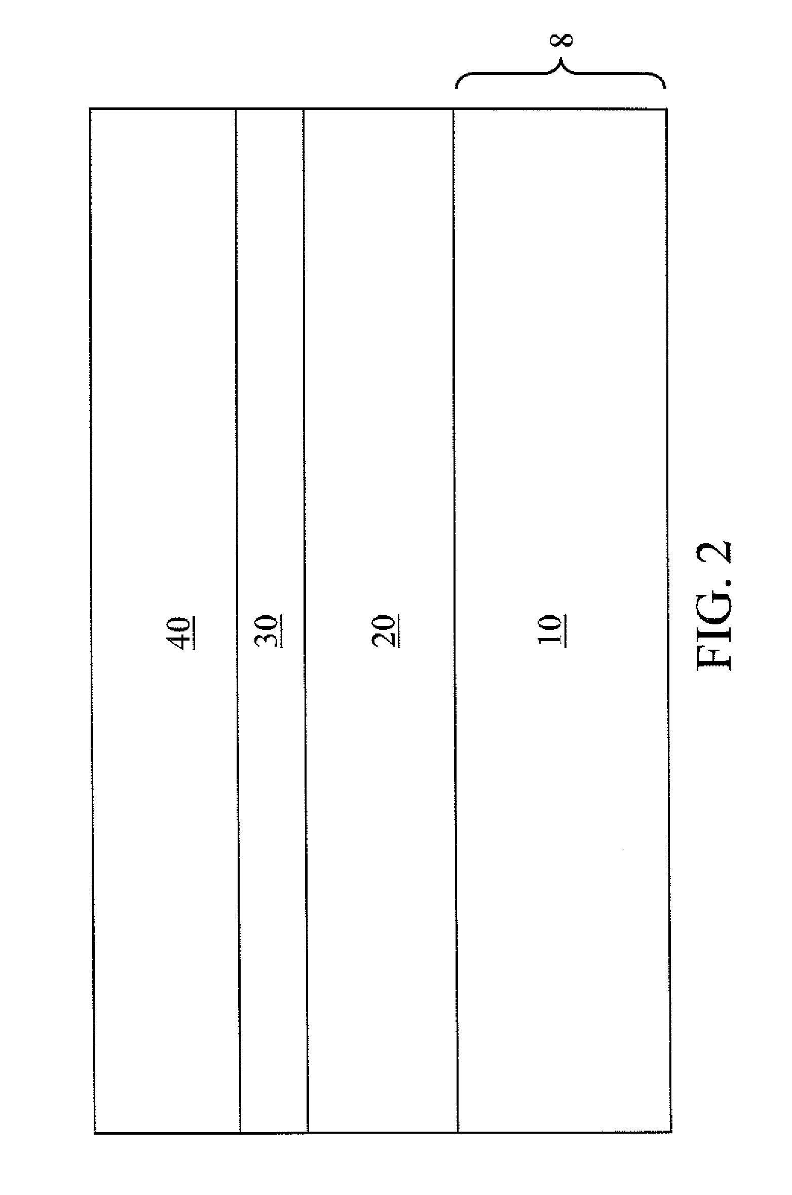
[0107]Referring to FIG. 4, a second exemplary semiconductor structure according to the present invention is derived from the first exemplary semiconductor structure of FIG. 2 by removing the metal aluminum nitride layer 30 and the semiconductor layer 40 by an etch, which may be a dry etch or a wet etch, that is selective to the mixed high-k material layer 20. The semiconductor layer 40 and the metal aluminum nitride layer 30 may be removed sequentially.

[0108]Referring to FIG. 5, a band edge metal layer 50 is formed by depositing a layer of metal that has Fermi level near the valence band edge of the semiconductor region 10 or near the conduction band edge of the semiconductor region 10. In case the semiconductor region 10 comprises silicon, the band edge metal layer 50 comprises a silicon valence band edge metal, i.e., a metal having a Fermi level near the valence band edge of silicon, or a silicon conduction band edge metal, i.e., a metal having a Fermi level near the conduction ba...

third embodiment

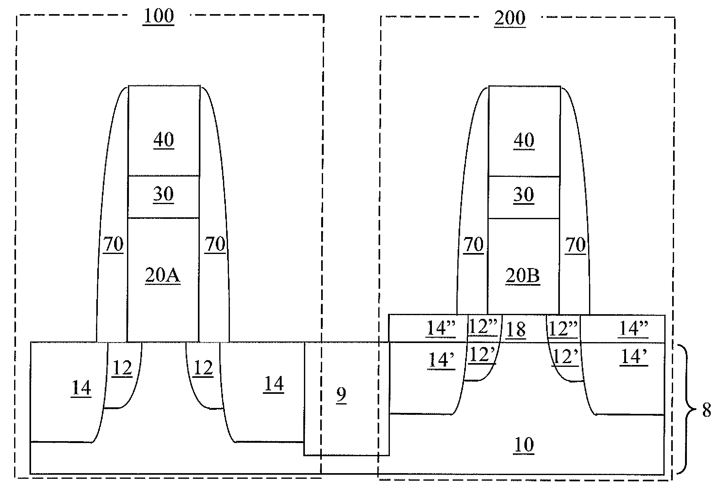
[0111]Referring to FIG. 7, a third exemplary semiconductor structure according to the present invention is derived from the first exemplary semiconductor structure of FIG. 2 by patterning the semiconductor layer 40, the metal aluminum nitride layer 30, and the mixed high-k material layer 20 by lithographic methods and a series of anisotropic etches. The remaining portions of the semiconductor layer 40, the metal aluminum nitride layer 30, and the mixed high-k material layer 20 collectively constitute a dummy gate stack (20, 30, 40). Source and drain extension regions 12 are formed in the semiconductor substrate 8 by implanting dopants into exposed regions of the semiconductor substrate 8. A dielectric spacer 170 is formed by conformal deposition of a dielectric material layer and an anisotropic reactive ion etch VIE). The dielectric spacer 170 comprises a dielectric material such as a dielectric oxide, a dielectric oxynitride, or a dielectric nitride. For example, the dielectric spa...


PUM


Abstract

A stack comprising a dielectric interface layer, a high-k gate dielectric layer, a group IIA/IIIB element layer is formed in that order on a semiconductor substrate. A metal aluminum nitride layer and, optionally, a semiconductor layer are formed on the stack. The stack is annealed at a raised temperature, e.g., at about 1,000° C. so that the materials in the stack are mixed to form a mixed high-k gate dielectric layer. The mixed high-k gate dielectric layer is doped with a group IIA/IIIB element and aluminum, and has a lower effective oxide thickness (EOT) than a conventional gate stack containing no aluminum. The inventive mixed high-k gate dielectric layer is amenable to EOT scaling due to the absence of a dielectric interface layer, which is caused by scavenging, i.e. consumption of any dielectric interface layer, by the IIA/IIB elements and aluminum.

Description

FIELD OF THE INVENTION[0001]The present invention generally relates to semiconductor devices, and particularly to semiconductor structures having a scalable high-k dielectric gate stack, and methods of manufacturing the same.BACKGROUND OF THE INVENTION[0002]High gate leakage current of silicon oxide and nitrided silicon dioxide as well as depletion effect of polysilicon gate electrodes limits the performance of conventional semiconductor oxide based gate electrodes. High performance devices for an equivalent oxide thickness (EOT) less than 1 nm require high dielectric constant (high-k) gate dielectrics and metal gate electrodes to limit the gate leakage current and provide high on-currents. Materials for high-k gate dielectrics include ZrO2, HfO2, other dielectric metal oxides, alloys thereof, and their silicate alloys.[0003]A high-k dielectric material needs to provide good electrical stability, that is, the amount of charge trapped in the high-k dielectric material needs to remain...

Claims


Application Information

Patent Timeline
IPC IPC(8): H01L27/088H01L29/78H01L21/28H01L21/8234
CPCH01L21/28088H01L21/28185H01L21/823807H01L29/66545H01L21/823864H01L29/517H01L21/823857
Inventor CHOI, CHANGHWANANDO, TAKASHICHOI, KISIKNARAYANAN, VIJAY
Owner SONY CORP
Why Eureka
Try Eureka