Infrared Source and Method of Manufacturing the Same

a technology of infrared source and manufacturing method, which is applied in the field of infrared source, can solve the problems of small number of components, inability to set specific wavelengths to arbitrary values, and few infrared sources capable of strong intensity, and achieves the effect of simple structur

Active Publication Date: 2009-05-21
NALUX CO LTD +1
View PDF4 Cites 35 Cited by
  • Summary
  • Abstract
  • Description
  • Claims
  • Application Information

AI Technical Summary

Benefits of technology

[0023]According to the present invention, the infrared source having a simple structure and radiating

Problems solved by technology

There are few infrared sources capable of obtaining strong intensity at a specific wavelength in an infrared wavelength range.
Although some of expensive lasers are oscillated at the specific wavelengths, the specific wavelengths cannot be set to arbitrary values.
However, such a device has problems that the number of components is large, a method of manufacturing a wavelength filter is complicated, and output energy is extremely low.
However, the high-temperature light emitting micro cavity light source has a complicated structure.
Actually, since this method is hard to obtain reliable results due to an influence of aging change, etc. of the elements or the optical system, in many cases some kind of reference signals are used.
Therefore, conventional analysis systems waste much energy and cannot reduce an outpu

Method used


Image

  • Infrared Source and Method of Manufacturing the Same
  • Infrared Source and Method of Manufacturing the Same
  • Infrared Source and Method of Manufacturing the Same

Examples


second embodiment

FIG. 22

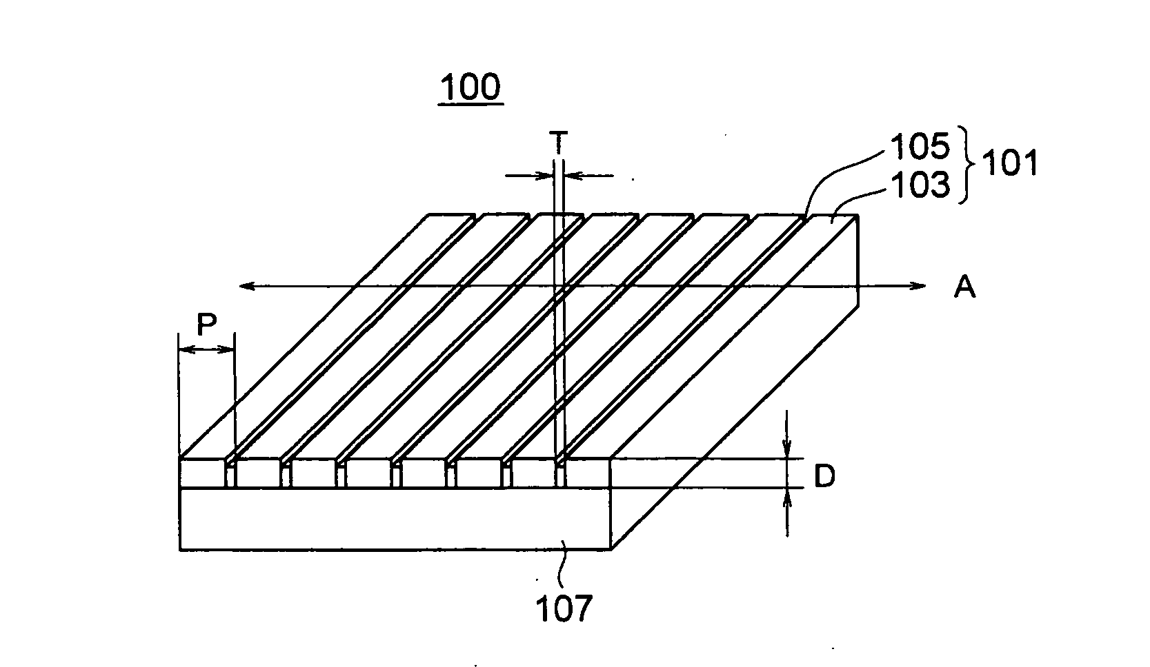
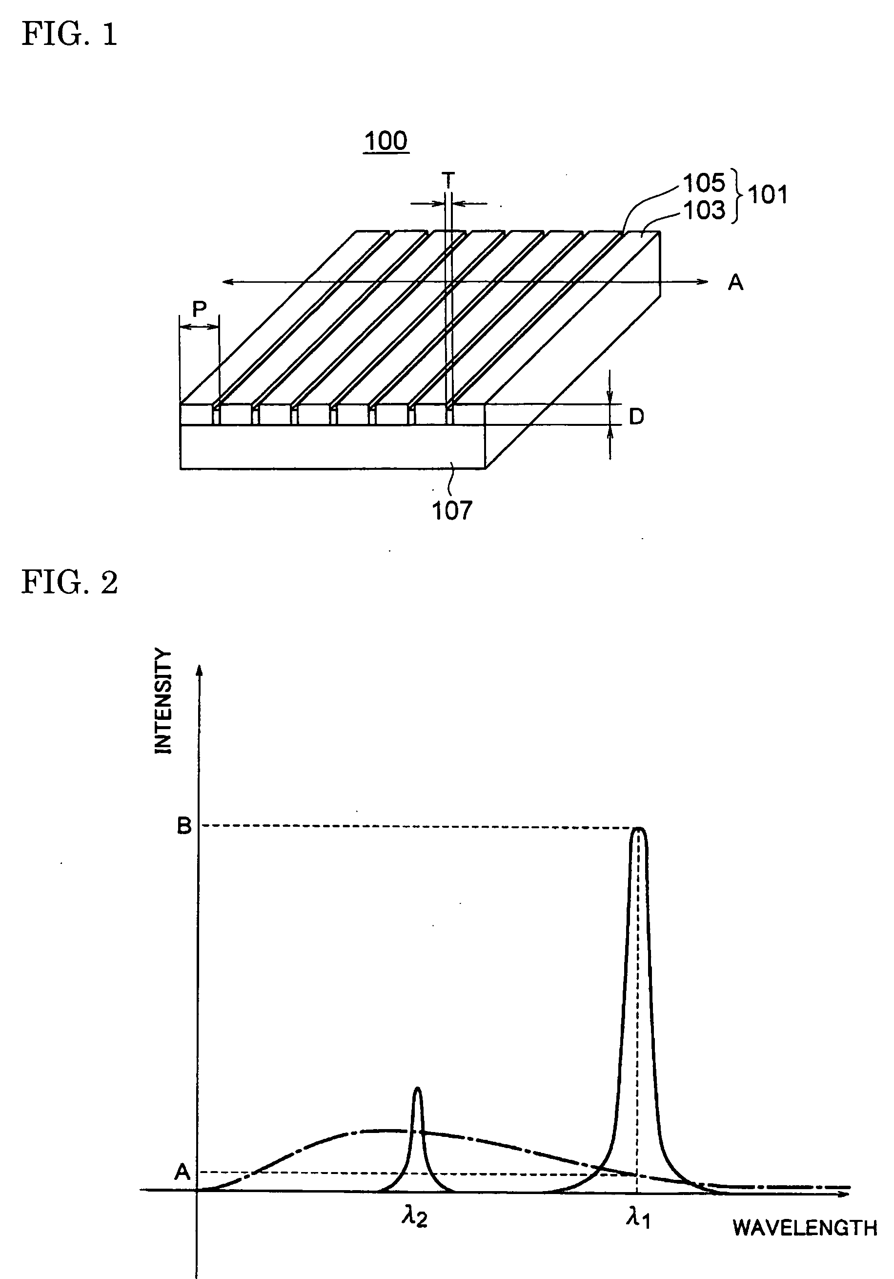
[0168]A resist (2b) is applied on a substrate (2a) (resin, metal, semiconductor, or the like; in the present embodiment, Si substrate) on which the grating portion is formed (FIG. 22(a)). Next, a grating pattern is formed by electron beam lithography, interference exposure, or mask exposure (FIG. 22(b)) and a projection array is manufactured by dry etching or the like (FIG. 22(c)). As a process of manufacturing the projection array, a nano imprinting technology may be used.

[0169]Subsequently, a film of Au (2c), or the like is formed on the projection array after removing the resist (FIG. 22(d)). At this time, a film thickness is preferably several times as large as a skin depth (20 to 30 nm in the case of Au) over all surfaces. As a film forming method, a vacuum deposition method or a sputtering method may be used. Especially, an atomic layer deposition (ALD) method by which extremely uniform film thickness can be obtained is effective. As methods by which a relatively thick ...

third embodiment

FIG. 23

[0180]In the present embodiment, a projection array is formed by transferring a mold (3b) having a surface on which a groove array is machined, on a surface of a substrate (3a) of thermoplastic resin or rubber (FIG. 23(a)). The mold can be manufactured by a method of applying the resist on the Si substrate and forming the grating pattern by electron beam lithography, interference exposure, mask exposure, or the like, a method of directly applying resist on the surface of the mold, forming the grating pattern by electron beam lithography, interference exposure, mask exposure, and forming a micro pattern by dry etching, or the like, a method of using a mechanical processing, or the like. A resin with heat resistance or the like may be used as the thermoplastic resin. Further, as the transfer method, an injection molding, a nano imprinting or the like can be used.

[0181]Next, a film of Au or the like (3c) is formed on a surface of the thermoplastic resin, or the like (FIG. 23(b))...

fourth embodiment

FIG. 24

[0190]In the present embodiment, a SOI substrate having a SiO2 layer (4b) formed on a Si substrate (4a) and a Si layer (4g) formed further thereon is used. A plane orientation of the Si layer (4g of FIG. 24) on the outermost surface is a 110 direction and its thickness is set to a depth of a grating to be manufactured. A resist (4c) is applied on the SOI substrate (FIG. 24(a)) and a grating pattern is formed thereon by electron beam lithography, interference exposure, mask exposure or the like (FIG. 24(b)). If it is etched with aqueous solution of KOH, the Si layer is etched in the direction perpendicular to its surface because etching speed varies depending on direction with respect to the crystal plane. Thereafter, when the etching reaches the SiO2 layer, the etching is terminated, so that the rectangular grating of Si is manufactured (FIG. 24(c)). Next, the resist is removed and a film of Au, etc. (4d) is then formed on the grating of Si (FIG. 24(d)). At this time, the fil...


PUM

PropertyMeasurementUnit
Lengthaaaaaaaaaa
Widthaaaaaaaaaa
Widthaaaaaaaaaa

Abstract

There is provided an infrared light source that has a simple structure and radiates infrared rays polarized in a specific direction and having a specific wavelength. The infrared light source (100) comprises a heat generator (107) and a latticework (101) in which a dielectric part (105) and a metal part (103) are alternately formed at a constant pitch in a constant direction. The infrared rays are radiated in a direction perpendicular to the surface of the latticework and are polarized in the direction indicated by an arrow A. If the constant pitch is denoted by P, the width of the dielectric part in the constant direction by T, and the specific wavelength by λ, for arbitrary P and T that meet the inequalities 0<P≦2.0 and T≦0.5P, the depth D of the latticework is so selected that the intensity spectrum of the infrared rays radiated from the infrared light source has the peak at λ.

Description

TECHNICAL FIELD[0001]The present invention relates to an infrared source that generates infrared light with a specific wavelength and a method of manufacturing the same. In particular, the present invention relates to an analysis system and a monitor system that use the infrared source.BACKGROUND ART[0002]There are few infrared sources capable of obtaining strong intensity at a specific wavelength in an infrared wavelength range.[0003]Although some of expensive lasers are oscillated at the specific wavelengths, the specific wavelengths cannot be set to arbitrary values.[0004]There is considered a device in which light with arbitrary wavelengths is taken out from radiant light radiated from a heater, etc. using a filter, or the like. However, such a device has problems that the number of components is large, a method of manufacturing a wavelength filter is complicated, and output energy is extremely low.[0005]Also, there has been proposed a high-temperature light emitting micro cavit...

Claims


Application Information

Patent Timeline
IPC IPC(8): G01J3/10B23P17/00
CPCG01J3/108Y10T29/49002H01K1/14G02B5/1809
Inventor INOUE, YASUAKIIKEDA, KATSUMOTOMIYAZAKI, HIDEKI
Owner NALUX CO LTD
Why Eureka
Try Eureka