Method for reversibly mounting a device wafer to a carrier substrate

a carrier substrate and device wafer technology, applied in the field of temporary wafer bonding methods, can solve the problems of high thermal and mechanical stress on the device wafer, the inability to form backside electrical contacts that connect with the front-side circuitry, and the thinned device wafers that have been less than 100 microns thinned,

Active Publication Date: 2009-09-03
BREWER SCI
View PDF70 Cites 211 Cited by
  • Summary
  • Abstract
  • Description
  • Claims
  • Application Information

AI Technical Summary

Benefits of technology

[0025]In a further embodiment, the invention is directed towards an article comprising a substrate having front and back surfaces. The front surface of the substrate has a peripheral region and a central region, and a layer of material is on the front surface at the central region. The layer is absent from the peripheral region and is selected from the group consisting of a low adhesive strength layer and a surface modification of the front surface.

Problems solved by technology

Without thinning, it would be nearly impossible to form backside electrical contacts that connect with front-side circuitry by passing the connections through the wafer.
Device wafers that have been thinned to less than 100 microns, and especially those thinned to less than 60 microns, are extremely fragile and must be supported over their full dimensions to prevent cracking and breakage.
Various wafer wands and chucks have been developed for transferring ultra-thin device wafers, but the problem still exists of how to support the wafers during back-grinding and TSV-formation processes that include steps such as chemical-mechanical polishing (CMP), lithography, etching, deposition, annealing, and cleaning, because these steps impose high thermal and mechanical stresses on the device wafer as it is being thinned or after thinning.
(1) Chemical—The bonded wafer stack is immersed in, or sprayed with, a solvent or chemical agent to dissolve or decompose the polymeric adhesive.
(2) Photo-Decomposition—The bonded wafer stack is irradiated with a light source through a transparent carrier to photo-decompose the adhesive boundary layer that is adjacent to the carrier. The carrier can then be separated from the stack, and the balance of the polymeric adhesive is peeled from the device wafer while it is held on a chuck.
(3) Thermo-Mechanical—The bonded wafer stack is heated above the softening temperature of the polymeric adhesive, and the device wafer is then slid or pulled away from the carrier while being supported with a full-wafer holding chuck.
(4) Thermal Decomposition—The bonded wafer stack is heated above the decomposition temperature of the polymeric adhesive, causing it to volatilize and lose adhesion to the device wafer and carrier.
Each of these debonding methods has drawbacks that seriously limit its use in a production environment.
For example, chemical debonding by dissolving the polymeric adhesive is a slow process because the solvent must diffuse over large distances through the viscous polymer medium to effect release.
Photo-decomposition is likewise a slow process because the entire bonded substrate cannot be exposed at one time.
The beam is then scanned (or rastered) across the substrate in a serial fashion to debond the entire surface, which leads to long debonding times.
While thermo-mechanical (TM) debonding can be performed typically in a few minutes, it has other limitations that can reduce device yield.
Backside processes for temporarily bonded device wafers often involve working temperatures higher than 200° C. or even 300° C. The polymeric adhesives used for TM debonding must neither decompose nor soften excessively at or near the working temperature, otherwise, debonding would occur prematurely.
At the same time, the high mechanical force required to move the device wafer away from the carrier by a sliding, lifting, or twisting motion creates additional stress that can cause the device wafer to break or produces damage within the microscopic circuitry of individual devices, which leads to device failure and yield loss.
Thermal decomposition (TD) debonding is also prone to wafer breakage.
The accumulation of trapped gases can cause the thin device wafer to blister and crack or even rupture.
Another problem with TD debonding is that polymer decomposition is often accompanied by the formation of intractable, carbonized residues that cannot be removed from the device wafer by common cleaning procedures.

Method used


Image

  • Method for reversibly mounting a device wafer to a carrier substrate
  • Method for reversibly mounting a device wafer to a carrier substrate
  • Method for reversibly mounting a device wafer to a carrier substrate

Examples


example 1

Edge Surface Adhesively Bonded and Center Surface Chemically Modified

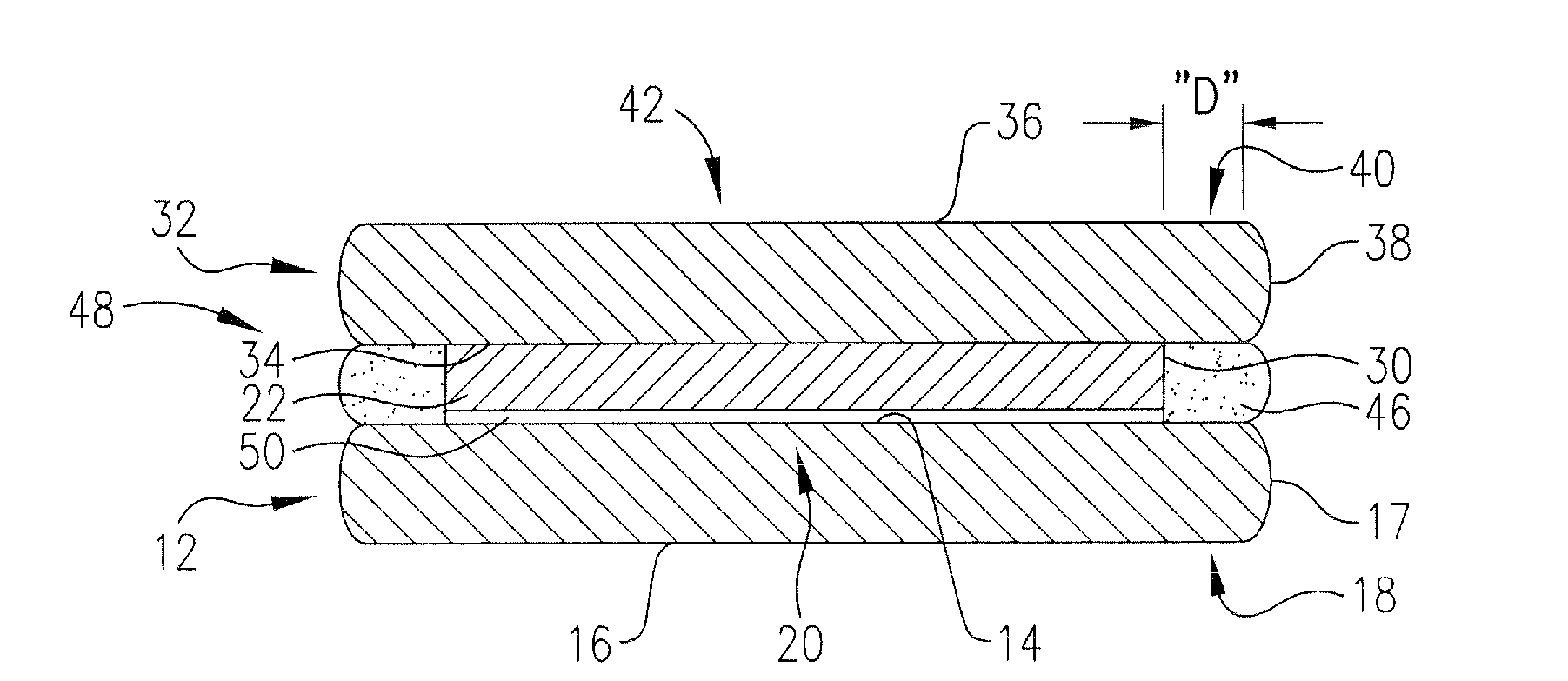
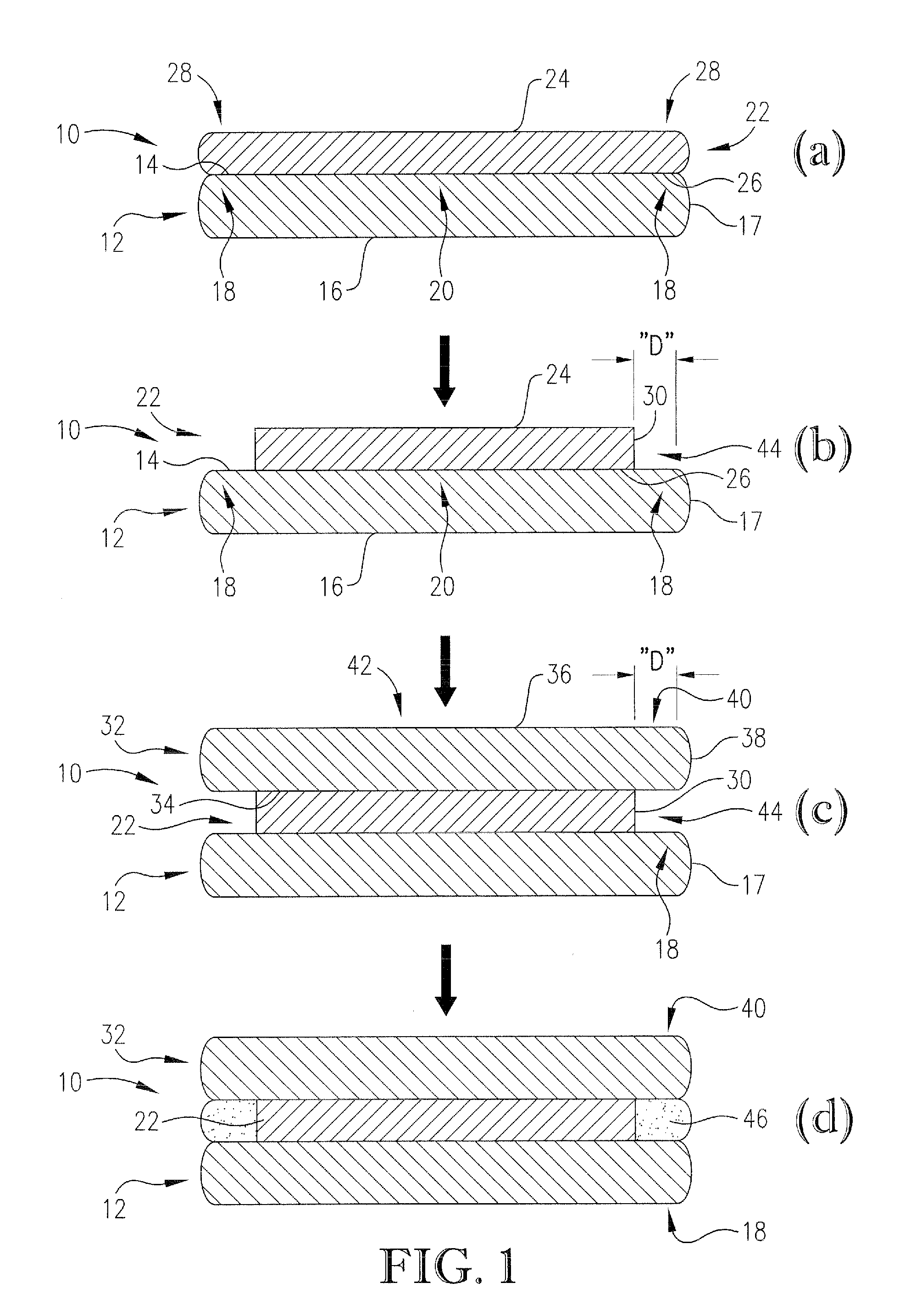
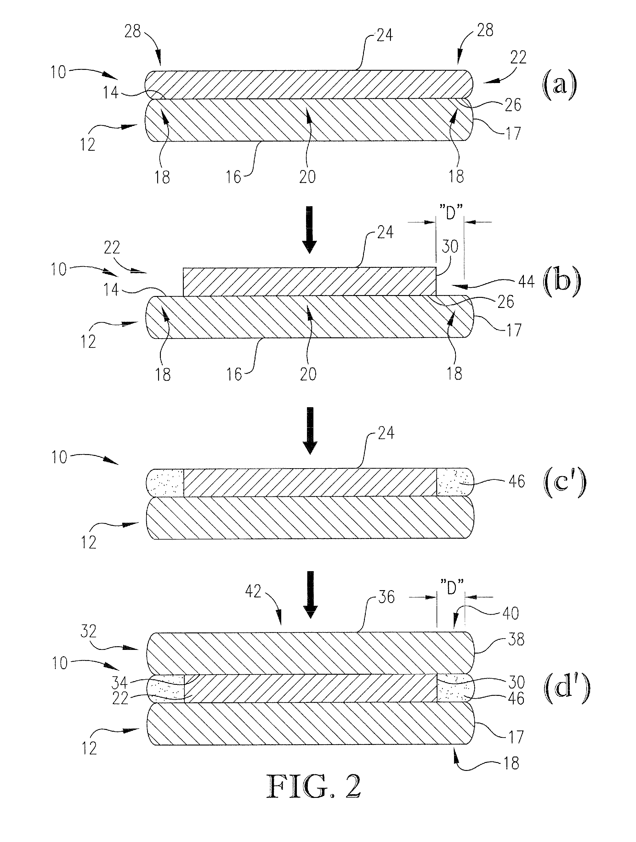
[0075]An epoxy-based photoresist (SU-8 2002, Microchem, Newton, Mass.) was dispensed onto the surface of a 100-mm silicon wafer (wafer 1) at the outer edge to coat a section of the wafer surface that was about 3-5 mm wide. A fluorinated silane ((heptadecafluoro-1,1,2,2-tetrahydrodecyl)trichlorosilane) was diluted to a 1% solution using FC-40 solvent (perfluoro compound with primarily C12, sold under the name Fluorinert, obtained from 3M). The solution was spin coated onto the surface of wafer 1. The wafer 1 was baked on a hotplate at 100° C. for 1 minute. It was rinsed with FC-40 solvent in a spin coater and baked at 100° C. for an additional 1 minute. The epoxy-based photoresist was removed using acetone in a spin coater, leaving the edge untreated from the fluorinated silane solution.

[0076]The surface of another 100-mm silicon wafer (wafer 2) was coated with a bonding composition (WaferBOND® HT 10.10, available f...

example 2

Edge Surface Adhesively Bonded, Center Surface Chemically Modified, and Debonding Using Solvent Jet at Edge with Wedge

[0077]An epoxy-based photoresist was dispensed onto the surface of a 200-mm silicon wafer (wafer 1) at the outer edge to coat a section of the wafer surface that was about 3-5 mm wide. A fluorinated silane ((heptadecafluoro-1,1,2,2-tetrahydrodecyl)trichlorosilane) was diluted to a 1% solution using FC-40 solvent. The solution was spin coated onto the surface of wafer 1. The wafer 1 was baked on a hotplate at 100° C. for 1 minute. It was rinsed with FC-40 solvent in a spin coater and baked at 100° C. for an additional 1 minute. The epoxy-based photoresist was removed using acetone in a spin coater, leaving the edge untreated from the fluorinated silane solution.

[0078]The surface of another 200-mm silicon wafer (wafer 2) was coated with WaferBOND® HT10.10 bonding composition via spin coating. This wafer was baked at 110° C. for 2 minutes and 160° C. for 2 minutes. The ...

example 3

Edge Surface Adhesively Bonded and Center Surface Coated with Release Material

[0079]A negative epoxy-based photoresist (sold under the name SU-8 2010, obtained from MicroChem) was spin coated onto the surface of a 100-mm glass wafer. The wafer was baked at 110° C. for 2 minutes. A Teflon® AF solution (Teflon® AF2400 in FC-40, obtained from DuPont) was spin coated over the SU-8 2010. Then, FC-40 solvent was dispensed onto the surface of the wafer at the outer edge to remove about a 3-5 mm wide section of the Teflon® AF coating from the wafer surface. The wafer was baked at 110° C. for 2 minutes. The wafer was bonded in a face-to-face relationship with a blank, 100-mm silicon wafer under vacuum at 120° C. for 3 minutes in a heated vacuum & pressure chamber. The bonded wafers were exposed to broadband UV light from the outer side of the glass wafer. The exposed wafers were baked at 120° C. for 2 minutes to crosslink the SU-8 2010 coating. They were debonded by inserting a razor blade a...


PUM

PropertyMeasurementUnit
widthaaaaaaaaaa
thicknessaaaaaaaaaa
diameteraaaaaaaaaa

Abstract

New temporary bonding methods and articles formed from those methods are provided. The methods comprise bonding a device wafer to a carrier wafer or substrate only at their outer perimeters in order to assist in protecting the device wafer and its device sites during subsequent processing and handling. The edge bonds formed by this method are chemically and thermally resistant, but can also be softened, dissolved, or mechanically disrupted to allow the wafers to be easily separated with very low forces and at or near room temperature at the appropriate stage in the fabrication process.

Description

RELATED APPLICATIONS[0001]The present invention claims the benefit of U.S. Provisional Application No. 61 / 023,379, filed Jan. 24, 2008, entitled METHOD FOR REVERSIBLY MOUNTING A DEVICE WAFER TO A CARRIER SUBSTRATE, incorporated by reference herein.BACKGROUND OF THE INVENTION[0002]1. Field of the Invention[0003]The present invention is broadly concerned with novel temporary wafer bonding methods that can support a device wafer on a carrier substrate during wafer thinning and other backside processing.[0004]2. Description of the Prior Art[0005]Integrated circuits, power semiconductors, light-emitting diodes, photonic circuits, microelectromechanical systems (MEMS), embedded passive arrays, packaging interposers, and a host of other silicon- and compound semiconductor-based microdevices are produced collectively in arrays on wafer substrates ranging from 1-12 inches in diameter. The devices are then separated into individual devices or dies that are packaged to allow practical interfac...

Claims


Application Information

Patent Timeline
Patent Type & Authority Applications(United States)
IPC IPC(8): H01L29/02H01L21/306H01L29/84H01L33/00H01L23/495H01L29/86H01L29/20H01L23/498B32B38/00B32B17/06B32B15/04B32B9/00
CPCH01L21/6835H01L21/6836H01L2221/68318H01L2221/68327H01L2221/6834H01L2924/0002H01L2924/19041H01L2924/00Y10T428/31678
Inventor FLAIM, TONY D.MCCUTCHEON, JEREMY
Owner BREWER SCI
Why Eureka
Try Eureka