Optoelectronic oscillator and pulse generator

Inactive Publication Date: 2009-09-10
FURUKAWA ELECTRIC CO LTD
View PDF12 Cites 17 Cited by
  • Summary
  • Abstract
  • Description
  • Claims
  • Application Information

AI Technical Summary

Benefits of technology

[0026]Objects of the present invention are to improve a conventional optoelectronic

Problems solved by technology

However, there are few proposals of the high purity clock generator for a high-speed optical interconnection decreasing a timing jitter.
In addition, further reduction of the timing jitter is required in higher clock frequency, but it is not easy to achieve.
Therefore, an electric circuit which multiplies the clock frequency such as a conventional liquid crystal-oscillator becomes unnecessary.
A lot of conventional OEOs use an optical fiber as an optical delay circuit, and it is difficult to integrate compactly due to the bending loss of the optical fiber.
Therefore, it has been thought that it is difficult to use an O

Method used


Image

  • Optoelectronic oscillator and pulse generator
  • Optoelectronic oscillator and pulse generator
  • Optoelectronic oscillator and pulse generator

Examples


first embodiment

The First Embodiment

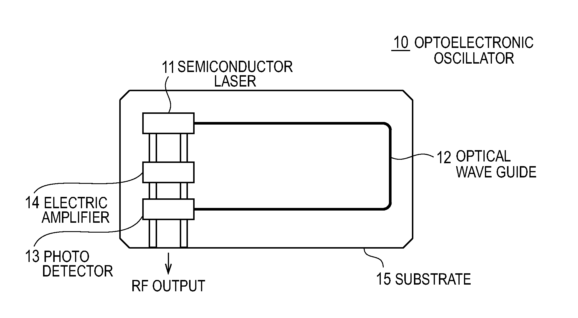
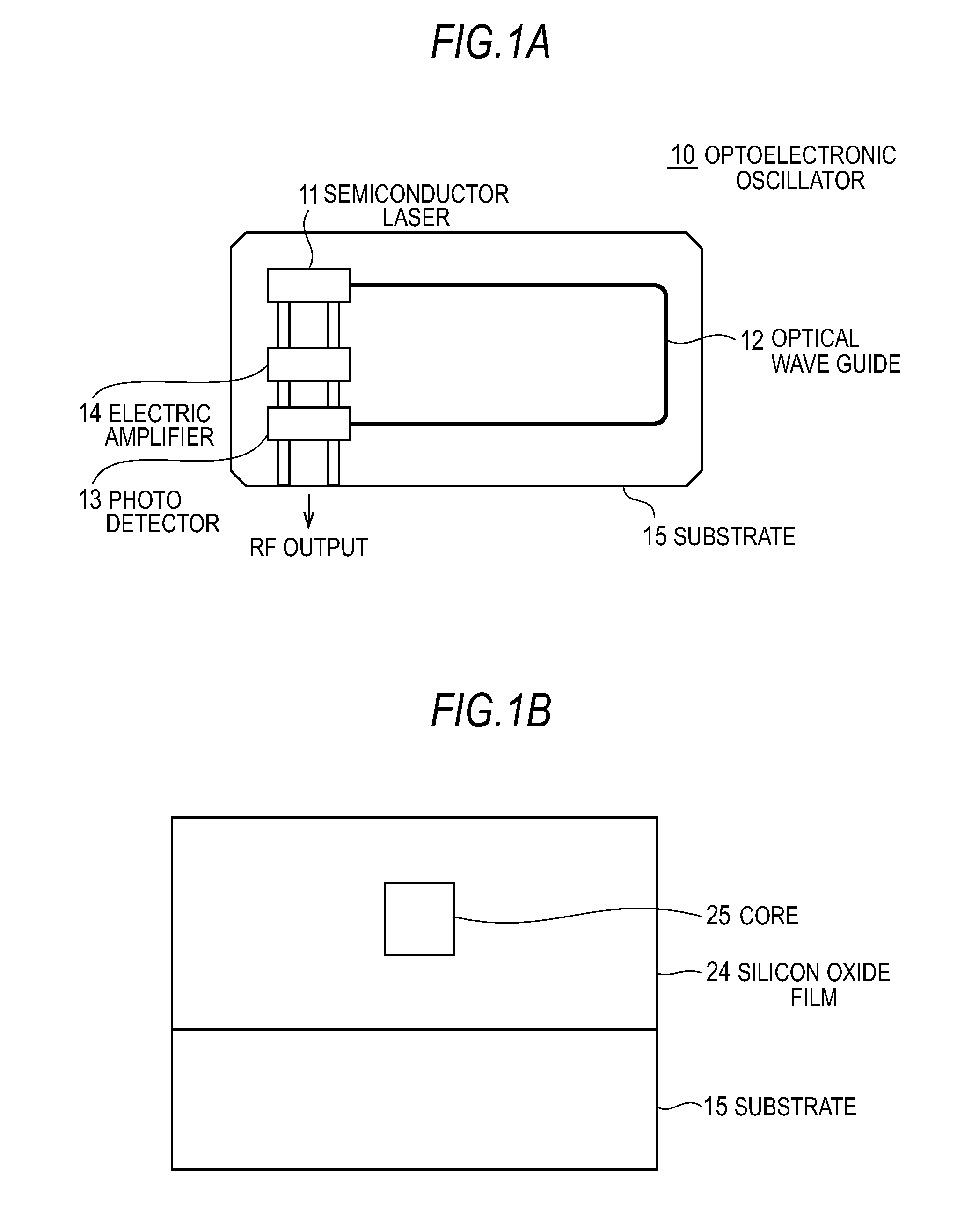
[0060]FIG. 1(a) shows an optoelectronic oscillator (hereinafter might be only called an oscillator) of the first embodiment of the present invention and FIG. 1(b) shows the section of an optical waveguide used in the optoelectronic oscillator. An oscillator 10 comprises a semiconductor laser (DFB laser) 11 as active element, a SiO2-system optical waveguide 12 as an optical delay circuit, a photodetector 13 containing InP compound semiconductor, and an amplifier 14 having a CMOS FET and constituent elements of the oscillator 10 are integrated on silicon substrate 15. As shown in FIG. 1(b), a silicon oxide film (SiO2) 24 is formed on a surface of the silicon substrate 15, in this silicon oxide film 24 germanium oxide (GeO2) is doped and a core 25 of the optical waveguide 12 is formed. In the present embodiment, the SiO2-system optical waveguide 12 is formed with embedded structure.

[0061]The DFB laser 11 is a semiconductor laser having oscillation wavelength of 1.55...

second embodiment

The Second Embodiment

[0066]The second embodiment of the present invention is applied to the process to manufacture the optoelectronic oscillator of the above described first embodiment. An optoelectronic oscillator monolithically forms a semiconductor laser, an optical waveguide and a photodetector on a compound semiconductor substrate such as InP. In the manufacture process, an active element part including active layer that will be a laser or a photodetector and a passive part that will be an optical waveguide are formed using butt joint growth method, for instance. The laser part and the photodetector constituting the active element part can be formed with embedded structure. Furthermore, the active layer uses 6 layers quantum well structure. The laser and the photodetector have the structures similar to the first embodiment. Furthermore, the optical waveguide part is formed with high mesa structure and its core, for instance, is formed with InGaAsP, and its thickness is 0.3 μm a...

third embodiment

The Third Embodiment

[0067]The third embodiment of the present invention is applied to the process to manufacture the optoelectronic oscillator of the above described first embodiment. The optoelectronic oscillator forms a laser and a photodetector on a SiO2-substrate by hybrid integration technology. In the manufacture process, a SiO2-substrate is formed through thermal oxidization of silicon and, for instance, high mesa waveguide of silicon is formed on the SiO2-substrate. High mesa structure is formed by RIE (Reactive Ion Etching) method using electron beam resist as a mask. For instance, its mesa depth is 0.2 μm and its mesa width is 1 μm, wave length, and the structure that it propagates in single mode at 1.55 μm is adopted. A semiconductor laser and a photodetector are aligned using active alignment or passive alignment technology using cross-shaped alignment mark and fixed on the SiO2-substrate using AuSn solder.


PUM


Abstract

The objects of the present invention are to shorten a cavity length of an optoelectronic oscillator and to integrate on a semiconductor or SiO2-substrate. An optoelectronic oscillator 10 have an optoelectronic loop comprising a semiconductor laser 11, an optical waveguide 12 guiding laser light emitted from the semiconductor laser, a photodetector 13 detecting laser light guided by the optical waveguide and outputting an electrical signal, an amplifier 14 amplifying the electrical signal outputted from the photodetector, generating an amplified signal and formed on a semiconductor substrate 15. Laser light emitted from the semiconductor laser 11 is controlled by generated amplified signal and it oscillates with a fundamental oscillation frequency determined by a delay time of carrier in the optoelectronic loop circuit or one of the high harmonic components of integral multiples of a fundamental oscillation frequency.

Description

CROSS-REFERENCE TO RELATED APPLICATIONS[0001]This application claims priority to Japanese patent application No. 2008-333148, filed on Dec. 26, 2008, and to Japanese patent application No. 2008-29069, filed on Feb. 8, 2008, the entire content of both of which are incorporated herein by reference.BACKGROUND OF THE INVENTION[0002]1. Field of the Invention[0003]This invention relates to an optoelectronic oscillator and a pulse generator, and more particularly to an especially preferred optoelectronic oscillator that can oscillate with a high frequency as an oscillator to generate a clock signal of CPU (Central Processing Unit) and a pulse generator having the optoelectronic oscillators.[0004]2. Description of the Related Art[0005]The clock frequency of the computer in recent years is high-speed such as about several GHz and it is important to accurately synchronize chips in order to have CPU work without malfunction. In order to synchronize accurately, decreasing an electromagnetic noi...

Claims


Application Information

Patent Timeline
IPC IPC(8): H01S5/026
CPCB82Y20/00G02B6/1223G02B2006/12121H01S5/06223G02B2006/1213G06F1/04G02B2006/12123
Inventor HASEGAWA, HIDEAKI
Owner FURUKAWA ELECTRIC CO LTD
Why Eureka
Try Eureka