Method for manufacturing soi substrate and method for manufacturing semiconductor device

Inactive Publication Date: 2009-10-01
SEMICON ENERGY LAB CO LTD
View PDF45 Cites 19 Cited by
  • Summary
  • Abstract
  • Description
  • Claims
  • Application Information

AI Technical Summary

Benefits of technology

[0021]According to one embodiment of the present invention, in manufacturing an SOI substrate or a semiconductor device, an SOI substrate having a single crystal semiconductor layer with reduced crystal defects can be manufactured. In addition, according to one embodiment of the present inven

Problems solved by technology

In the case where a single crystal semiconductor film is formed using the ion implantation separation method, defects in the single crystal semiconductor film is increased due to the addition of ions.
For example, in the case where there are a large number of defects in the single crystal semiconductor film, a defect level is easily formed at an interface with a gate insulating layer; therefore, characteristics of a semiconductor element formed using this single crystal semiconductor film is not good.
In addition, crystallinity and planarity are impaired

Method used


Image

  • Method for manufacturing soi substrate and method for manufacturing semiconductor device
  • Method for manufacturing soi substrate and method for manufacturing semiconductor device
  • Method for manufacturing soi substrate and method for manufacturing semiconductor device

Examples


embodiment mode 1

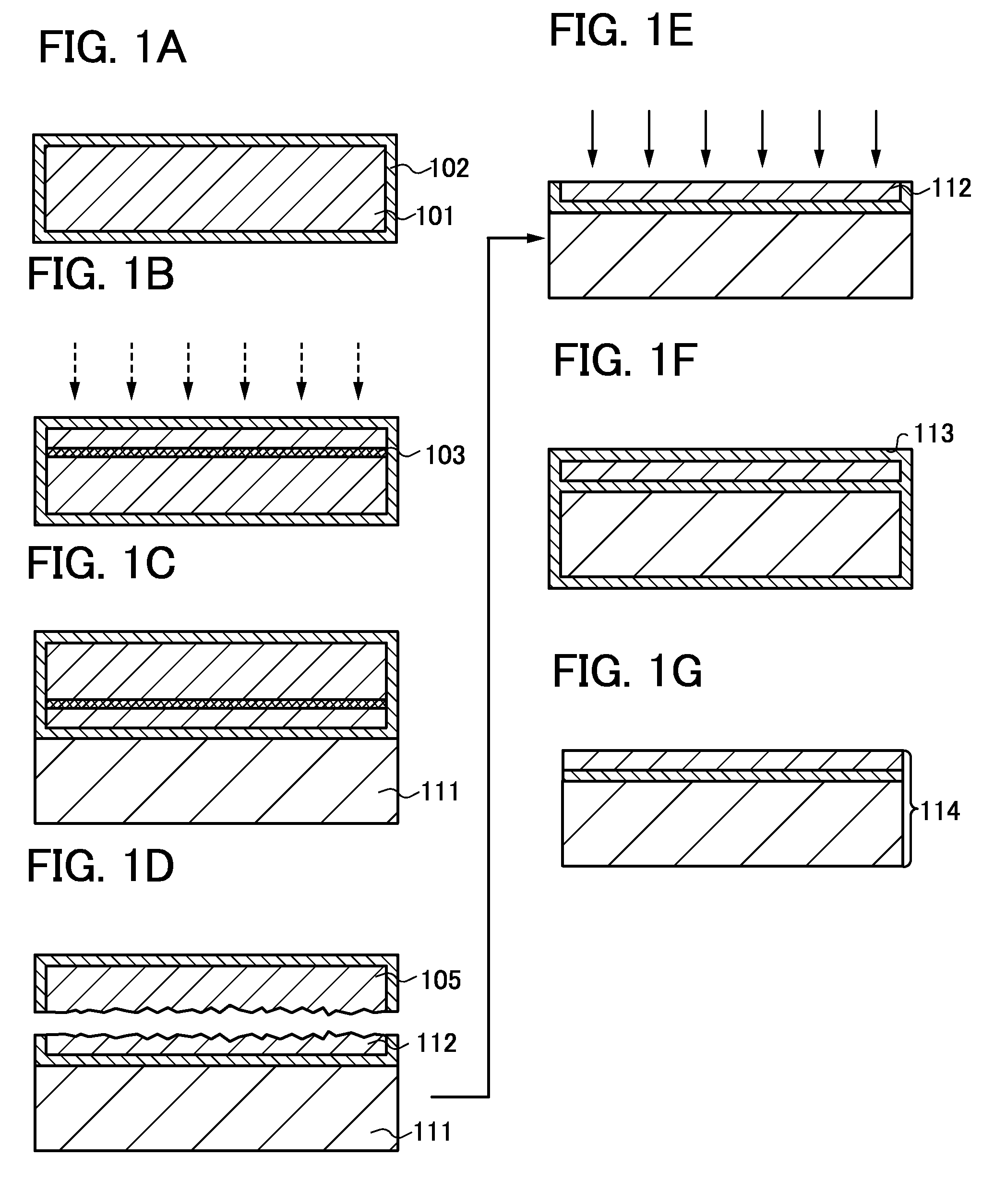
[0048]In this embodiment mode, an example of a method for manufacturing an SOI substrate will be described with reference to drawings.

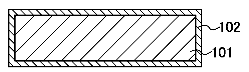
[0049]First, a single crystal semiconductor substrate 101 is prepared and washed using a sulfuric acid / hydrogen peroxide mixture (SPM), an ammonium hydroxide / hydrogen peroxide mixture (APM), a hydrochloric acid / hydrogen peroxide mixture (HPM), dilute hydrogen fluoride (DHF), ozone water, or the like as appropriate. As the single crystal semiconductor substrate 101, a commercial single crystal semiconductor substrate can be used. For example, a single crystal silicon substrate, a single crystal germanium substrate, and a compound semiconductor substrate of gallium arsenide, indium phosphide, or the like can be used. A size of a commercial silicon substrate is typically 5 inches (125 mm) in diameter, 6 inches (150 mm) in diameter, 8 inches (200 mm) in diameter, 12 inches (300 mm) in diameter, or 18 inches (450 mm) in diameter, and a typical shape thereo...

embodiment mode 2

[0156]This embodiment mode describes a method for manufacturing an SOI substrate, which is different from that in the above embodiment mode, with reference to drawings. Specifically, a case is described in which an SOI substrate is manufactured using a single crystal semiconductor substrate which has rounded corners (end portions) (with edge roll-off (ERO)). In addition, a case is described in which the single crystal semiconductor substrate is repeatedly used (reused) with reference to drawings.

[0157]First, the single crystal semiconductor substrate 101 (here, a single crystal silicon substrate) which has the oxide film 102 on its surface and the embrittlement region 103 in a region at a predetermined depth from its surface is prepared (see FIG. 16A). The detailed description of FIG. 16A is omitted because the method illustrated in FIGS. 1A and 1B may be employed.

[0158]In this embodiment mode, corners (end portions) of the single crystal semiconductor substrate 101 each have a roun...

embodiment mode 3

[0171]In this embodiment mode, a method for manufacturing the semiconductor device using the SOI substrate formed in Embodiment Mode 1 or Embodiment Mode 2 will be described. Here, an example of manufacturing a CMOS structure as the semiconductor device will be described with reference to FIGS. 17A to 17E. The same portions in FIGS. 17A to 17E as those of FIGS. 1A to 1G, FIGS. 2A and 2B, FIGS. 3A to 3F, FIGS. 4A to 4C, FIG. 5, FIG. 6, FIG. 7, FIG. 8, FIG. 9, FIG. 10, FIG. 11, FIG. 12, FIG. 13, FIG. 14, FIG. 15, and FIGS. 16A to 16I are denoted by the same reference numerals, and will not be further described.

[0172]With the use of the manufacturing method described in the above embodiment mode, the single crystal semiconductor layer 112 of the SOI substrate can be formed to a thickness of 100 nm or less. When the single crystal semiconductor layer 112 has a thickness of 100 nm or less, it is thinner than the maximum depth of a depletion layer in a channel formation region of a transi...


PUM


Abstract

A method for manufacturing an SOI substrate in which crystal defects of a single crystal semiconductor layer are reduced is provided. An oxide film containing halogen is formed on each of surfaces of a single crystal semiconductor substrate and of a semiconductor substrate provided with a single crystal semiconductor layer separated from the single crystal semiconductor substrate, whereby impurities that exist on the surfaces of and inside the substrates are decreased. In addition, the single crystal semiconductor layer provided over the semiconductor substrate is irradiated with a laser beam, whereby crystallinity of the single crystal semiconductor layer is improved and planarity is improved.

Description

BACKGROUND OF THE INVENTION[0001]1. Field of the Invention[0002]The present invention relates to a method for manufacturing an SOI substrate having a semiconductor layer formed over an insulating film and a method for manufacturing a semiconductor device.[0003]2. Description of the Related ArtBackground Art [0004]In recent years, instead of a bulk silicon wafer, integrated circuits using an SOI (silicon on insulator) substrate have been developed. By utilizing the characteristics of a thin silicon wafer formed over an insulating film, semiconductor layers of transistors formed in the integrated circuit can be separated from each other completely. Further, since the fully depleted transistors can be formed, a semiconductor integrated circuit with high added value such as high integration, high speed driving, and low power consumption can be realized.[0005]Known examples of SOI substrates are SIMOX substrates and bonded substrates. For example, an SOI structure of a SIMOX substrate is...

Claims


Application Information

Patent Timeline
IPC IPC(8): H01L21/477H01L21/46
CPCH01L21/76254
Inventor YAMAZAKI, SHUNPEINISHIDA, ERIKOSHIMAZU, TAKASHI
Owner SEMICON ENERGY LAB CO LTD
Why Eureka
Try Eureka