Inductively coupled coil and inductively coupled plasma device using the same

a technology of inductively coupled coils and plasma devices, which is applied in the direction of transformers/inductance coils/windings/connections, plasma techniques, etc., can solve the problems of non-uniformity of plasma density from the center to the periphery, non-uniformity of deposited power, and non-uniformity of ionization, so as to improve the uniformity of etching rate and other etch results, the effect of little differen

Active Publication Date: 2009-12-24
BEIJING NAURA MICROELECTRONICS EQUIP CO LTD
View PDF10 Cites 17 Cited by
  • Summary
  • Abstract
  • Description
  • Claims
  • Application Information

AI Technical Summary

Benefits of technology

[0009]The present invention is directed to solve at least one of the problems existing in the prior art, i.e., to provide an inductively coupled coil and an inductively coupled plasma device. Based on the inductively coupled coil of the present invention the plasma is uniformly distributed above a wafer in a reaction chamber due to an internal coil and an external coil configured by a plurality of respective branches and combination of the internal coil and external coil, so that there is little difference among chemical reaction rate of different area on the wafer surface. In addition, etch rate uniformity and other etch results are improved accordingly.
[0026]From the solutions disclosed above, since there is an internal coil and an external coil which are separated from each other and coaxially arranged with each other, the structures of the internal coil and the external coil in the inductively coupled coil and the inductively coupled plasma device can be designed as required, so as to achieve desired electromagnetic field. Further, because the internal coil and the external coil are consist of a plurality of respective branches that are substantially the same and nested together respectively and the respective branches are symmetrically connected in parallel, the inductance of the inductively coupled coil is reduced, and plasma with larger area can be easily obtained, thus ameliorating the uniformity of the plasma in large area process. Meanwhile, the electromagnetic field in the reaction chamber distributes uniformly due to the structure of the inductively coupled coil, and the plasma distributes more uniformly from the center to periphery thereof.

Problems solved by technology

Asymmetry of gas flow results in asymmetry of plasma conductivity, and the asymmetry of plasma conductivity may lead to non-uniformity of deposited power, which may lead to non-uniformity of ionization due to electron colliding.
And the non-uniformity of plasma density from the center to periphery becomes more serious.
Therefore, there is a problem in non-uniformity of etching rate for most of conventional etching apparatuses, which brings negative influence on the semiconductor manufacturing process.
However, the plasma excited by this configuration is very non-uniform.
This may lead to a small adjustable window to the process and great limitations to the semiconductor manufacturing process.
When the plasma density distributes uniformly, the etched depth on the wafer or the thickness of the material deposited on the wafer is non-uniform, thus the yield of the devices is also decreased.
Especially, when the diameter of the wafer increases from 100 mm to 300 mm, the volume of the reaction chamber increases correspondingly, and it is impossible to obtain uniform plasma density via diffusion.
The dielectric window 1 having such an thickness will lead to decrease of energy coupling efficiency, since there is no enough flux density to excite plasma after the RF field penetrating through the thick dielectric window 1.
And the problem with the conventional spiral inductively coupled coil is the generation of non-uniform plasma density.
Thus, the transmission line effect of the inductively coupled coil is obvious, and there exists remarkable variations of current and voltage in the inductively coupled coil, which results in remarkable variation of the magnetic flux density in the plasma and non-uniformity of workpiece processing.
The increased voltage will result in capacitive coupling between the inductively coupled coil and the plasma, and the capacitive coupling increases the kinetic energy of the ion, so that it is hard to control the process precisely.
In addition, it will increase micro-loading effect of the wafer and decrease yield of the devices.
Further, ions with relatively high kinetic energy collide with the inner walls of the plasma chamber, which will result in particle contamination.
And increased inductance will also lead to unstable impedance match and low coupling efficiency.

Method used


Image

  • Inductively coupled coil and inductively coupled plasma device using the same
  • Inductively coupled coil and inductively coupled plasma device using the same
  • Inductively coupled coil and inductively coupled plasma device using the same

Examples


first embodiment

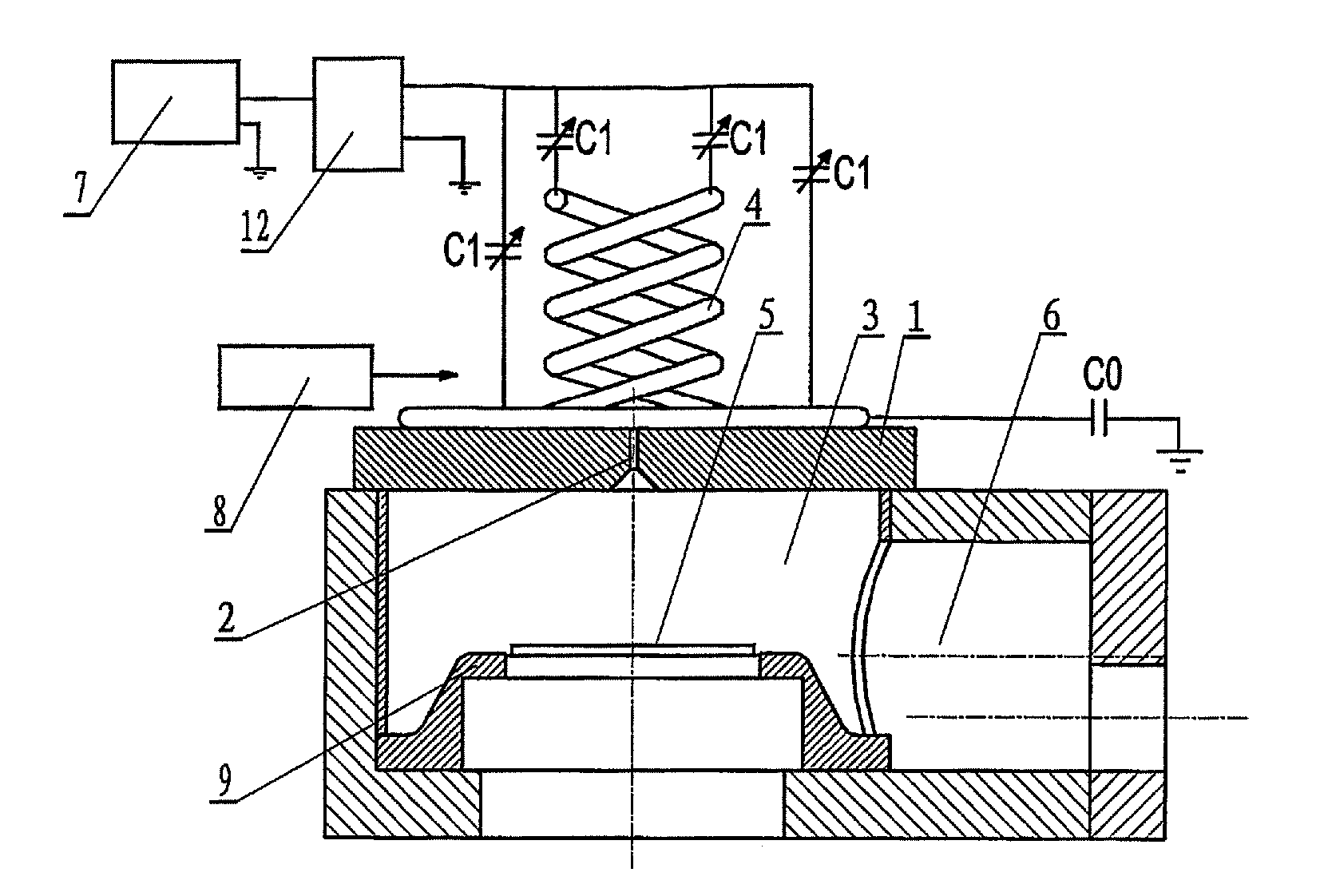
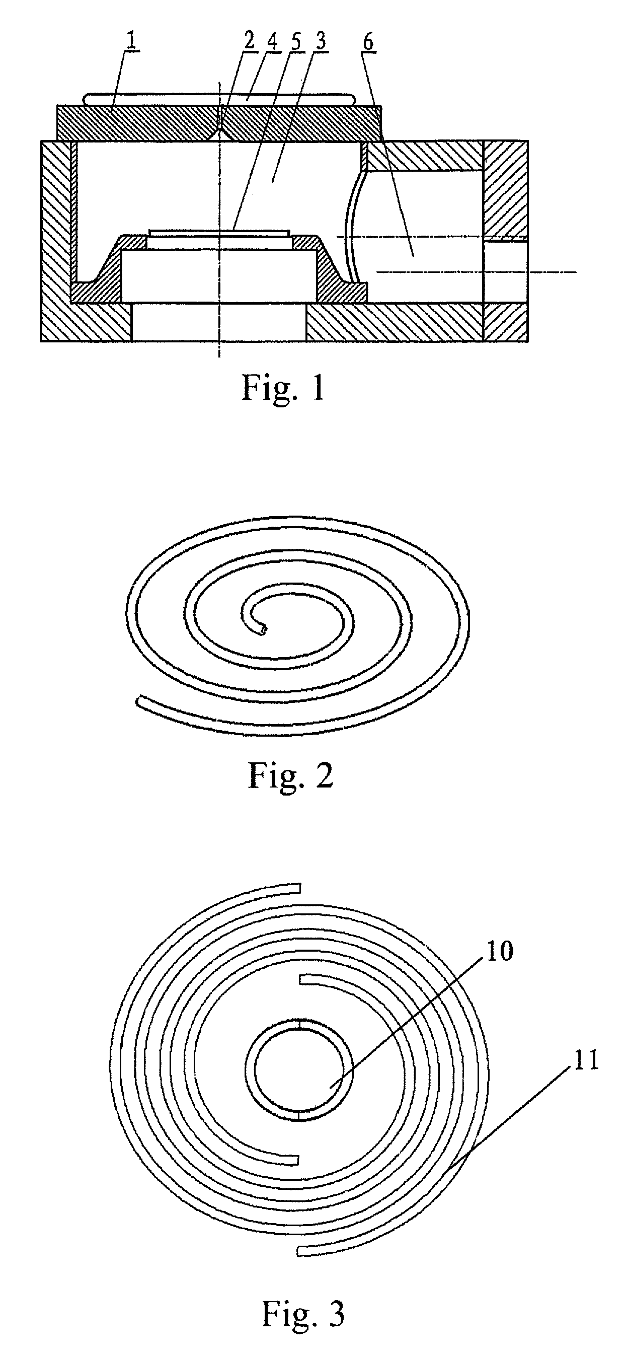
[0050]FIG. 7 shows an inductively coupled plasma device according to the invention in which the inductively coupled coil described above is applied. The inductively coupled plasma device comprises: a reaction chamber 3, a chuck 9 provided in the reaction chamber 3 for holding a wafer 5; and a dielectric window 1 provided at an top portion of the reaction chamber 3, an inlet 2 is provided at the middle part of the dielectric window 1, and processing gas is introduced into the reaction chamber 3 through the gas inlet 2 by a gas introducing device 8.

[0051]An inductively coupled coil 4 is provided on top of the dielectric window 1, and an input end of the inductively coupled coil 4 is connected with a RF (Radio Frequency) source 7 by a match 12. An output end of the inductively coupled coil 4 is grounded via a grounding capacitor C0. When an induced electric field is generated in the reaction chamber 3, the gas entering into the reaction chamber 3 is excitated into plasma for etching th...

second embodiment

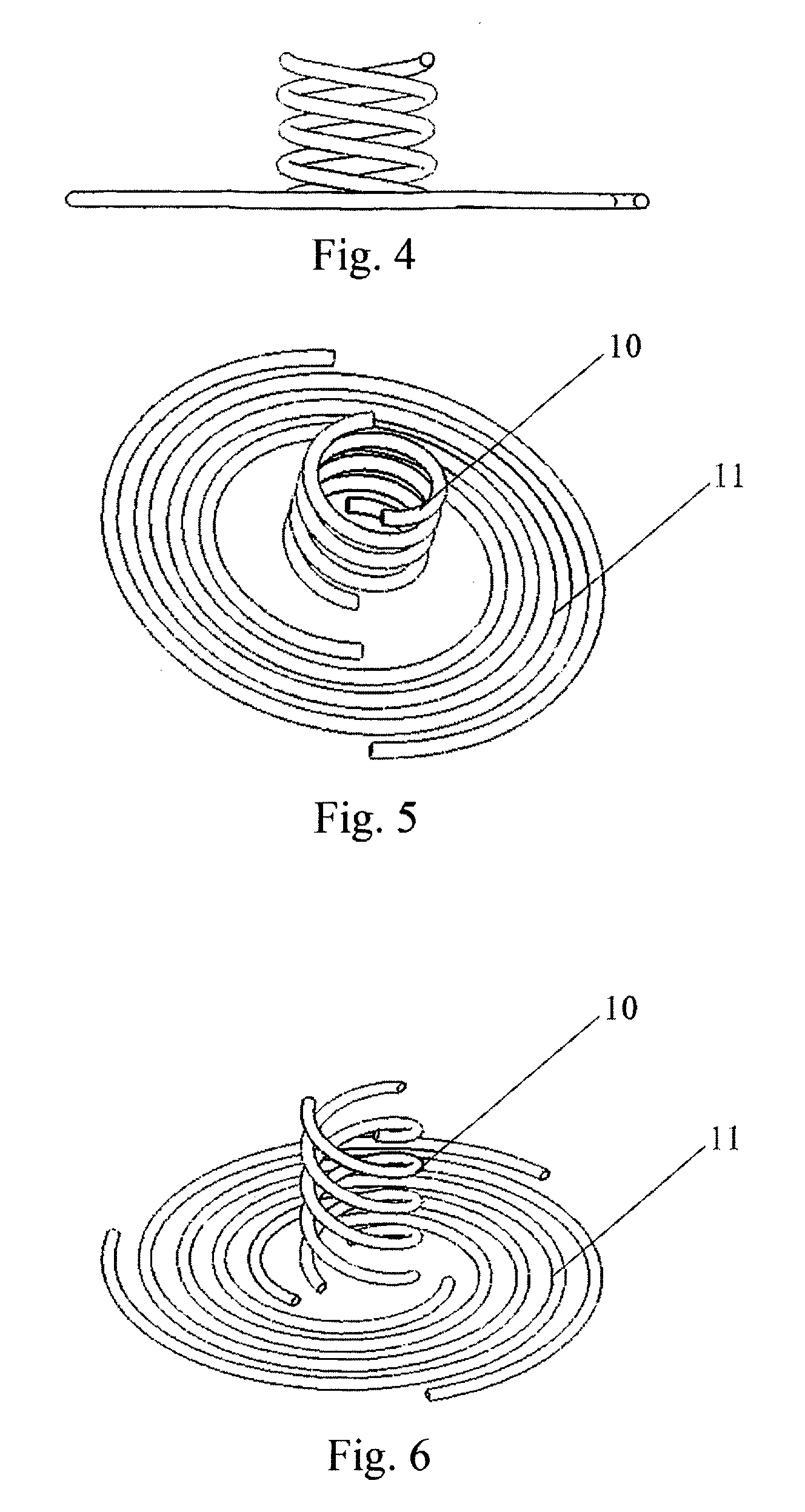
[0054]FIG. 8 shows an inductively coupled plasma device of the invention in which the inductively coupled coil described above is applied. The plurality of internal respective branches of the internal coil 10 in the inductively coupled coil are connected in parallel, and the input ends thereof are connected to an variable capacitor C1, then connected with the RF (radio frequency) source 7 via a match 12. The plurality of external respective branches of the external coil 11 in the inductively coupled coil are connected in parallel, and the input ends thereof are connected to an variable capacitor C1, then connected with the RF (radio frequency) source 7 via the match 12.

[0055]FIG. 9 shows an inductively coupled plasma device according to second embodiment of the invention in which the inductively coupled coil described above is applied. The plurality of internal respective branches of the internal coil 10 in the inductively coupled coil are connected in parallel, then connected with...


PUM

PropertyMeasurementUnit
frequencyaaaaaaaaaa
sizeaaaaaaaaaa
planar structureaaaaaaaaaa

Abstract

The present invention discloses an inductively coupled coil and an inductively coupled plasma device using the same. The inductively coupled coil comprises an internal coil and an exterior coil which are respective from each other and coaxially arranged, internal coil comprising a plurality of internal respective branches having the same configurations which are nested together, the plurality of internal respective branches being arranged symmetrically with respect to an axis of the inductively coupled coil; the external coil comprising a plurality of external respective branches having the same configurations which are nested together, the plurality of external respective branches being arranged symmetrically with respect to the axis of the inductively coupled coil. The inductively coupled coil is located on the reaction chamber of the inductively coupled plasma device and is connected to a RF source. It can make the plasma distribute uniformly on the wafer in the reaction chamber so that the difference in chemical reaction rate on the surface of the wafer is small and the quality of the etched wafer is improved. They can be applied in a semiconductor wafer manufacturing apparatus, and they can also be adapted to other apparatuses.

Description

BACKGROUND OF THE INVENTION[0001]1. Field of the Invention[0002]The present invention relates to an assembly for a semiconductor wafer manufacturing apparatus, more specially, to an inductively coupled coil and an inductively coupled plasma device using the same.[0003]2. Description of the Related Art[0004]Currently, with high development of electronic technology, there is stricter demand on integration level of IC, thus, IC enterprises have to improve manufacturing process of semiconductor wafers continuously. Plasma apparatuses or devices are widely used in manufacturing process of IC (Integrated Circuit) or MEMS (Micro-Electro-Mechanical System) devices. ICP (Inductively coupled plasma device) is widely used in etch process etc. Plasma is generated by RF gas ionization under low pressure. The plasma contains a large number of active particles such as electrons, ions, atoms, excited molecules and free radical etc. There occur chemical and physical reactions between these active pa...

Claims


Application Information

Patent Timeline
Patent Type & Authority Applications(United States)
IPC IPC(8): H01L21/465H01F5/00H01F38/14H01F27/28
CPCH01F38/10H01J37/321H01F38/14H01J37/3211H01J37/32119H01J37/32183H01L21/3065H05H1/24H05H1/46H01F27/28H01J2237/3344
Inventor SONG, QIAOLINAN, JIANHUI
Owner BEIJING NAURA MICROELECTRONICS EQUIP CO LTD
Why Eureka
Try Eureka