Thin film lamination, thin film magnetic sensor using the thin film lamination and method for manufacturing the thin film lamination

a thin film, magnetic sensor technology, applied in the direction of instruments, galvano-magnetic devices, transportation and packaging, etc., can solve the problems of high temperature dependence of resistance and electron mobility, marked characteristic deterioration, and difficult fabrication of highly sensitive magnetic sensors, so as to reduce the al component, increase the corrosion resistance of the buffer layer, and high resistance

Inactive Publication Date: 2010-02-25
ASAHI KASEI KK
View PDF3 Cites 33 Cited by
  • Summary
  • Abstract
  • Description
  • Claims
  • Application Information

AI Technical Summary

Benefits of technology

[0108]The foregoing is the description made by way of example that limits the buffer layer 2 to only AlInSb. However, it is not limited to the composition, and the buffer layer 2 of AlGaInSb obtained by adding Ga can also be employed, which also falls within the technical scope of the present invention. More specifically, although the Al composition in the buffer layer increases with an increase of the ratio of the As composition in the InAsSb thin film conducting layer, it is also possible to use a buffer layer adjusted to achieve the lattice matching with the InAsSb by adding Ga in a range without losing insulation. Adding Ga has merits in reducing the Al component, and an increase of the corrosion resistance of the buffer layer is expected.
[0109]Next, as for the substrates employed in the present invention, some of them other than GaAs will be described. It is enough for the substrate 1 used in the present invention to have heat resistance and insulation. It is not limited to a GaAs single crystal substrate. In addition, as long as an insulating or high resistance AlxGayIn1-x-ySb mixed crystal layer can be grown on it, its insulation is not necessarily important in particular.
[0110]In the present invention, the substrate 1 is normally composed of a material which is stable at high temperature, and a substrate having insulation or high resistance and a flat surface is used. Accordingly, an insulating single crystal substrate, which can provide a crystal face with a flat surface, is preferably used. In particular, insulating substrates composed of GaAs, InP or the like are preferably used. Alternatively, any substrates will do as long as they have an insulating or high resistance thin layer formed on their surfaces, and are substantially equivalent to a substrate having a flat surface composed of a thin layer formed with insulation or high resistance.
[0111]In addition, a Si single crystal substrate having a thin insulating layer formed on its surface is also used as the substrate 1 because an insulating flat surface with the same crystal structure as a GaAs substrate, a GaAs insulating compound semiconductor layer can be obtained by further placing on its surface. A sapphire substrate with good insulation is also preferable.
[0112]Next, the surface of the substrate must be flat. The term “flat” here refers to a state in which the surface asperities are 5 nm or less, and more preferably 1 nm or less, and in the optimum case, to a state in which the crystal lattice plane consisting of atoms constituting the substrate is arranged in a flatness of a single atom layer on the surface of the substrate in parallel with the lattice plane, that is, the substrate is a single crystal substrate and has a flatness equal to or less than a single atom layer consisting of the crystal lattice plane. Alternatively, a flatness equal to or less than the spacing of a single lattice plane is the most desirable flatness.
[0113]As for the substrate, it does not matter in particular whether it is a single crystal, polycrystal or in an amorphous state as long as it has insulation or high resistance. However, a single crystal with the same crystal structure as InAsSb is optimum, and further III-V compound semiconductor single crystal is desirable, and an insulating or semiconductor substrate such as GaAs, InP or GaN is preferable.

Problems solved by technology

As a result, fabrication of highly sensitive magnetic sensor is very difficult.
Besides, there is another problem of marked characteristic deterioration in a practical magnetic sensor manufacturing process.
In addition, a narrow band gap material such as InSb has an essential, very important problem in that although it has large electron mobility, its resistance and electron mobility has great temperature dependence.
Thus, it is necessary to protect the elements from damages due to over current, which imposes great restrictions on driving conditions, and presents a historically well-known problem in that the element driving becomes very difficult.
Furthermore, the large electron mobility will reduce the sheet resistance of the operating layer.
Accordingly, the electron mobility reduces with the reduction of the film thickness, and the formation of the operating layer for fabricating the highly sensitive magnetic sensor becomes impossible.
It presents a more serious problem than the layer with the low electron mobility, which results from the exposure of the surface of the operating layer to a vacuum or air, and becomes a cause of hampering the fabrication of a practical highly sensitive magnetic sensor.
Such surface damage to the operating layer occurring at the protective film formation takes place because of collision of atoms or molecules, which come flying at the protective film formation and constitute the protective film, with the surface of the operating layer with kinetic energy as well as because of the lattice mismatch between the protective film and the operating layer or the difference in the crystal structure between the protective film and the operating layer, and presents a very serious problem yet to be solved.
In addition, the damage reduces the reliability of the elements markedly, and increases variations of the characteristics of the elements fabricated.
Furthermore, there is a very serious problem of being unable to use the thin film of the operating layer for fabricating practical highly sensitive magnetic sensors.
It becomes a very difficult problem when trying to fabricate highly reliable practical magnetic sensors.
However, the technologies up to now do not implement such thin film lamination.
In particular, it is very difficult to fabricate highly sensitive, low power consumption, very small temperature dependence thin film magnetic sensors such as Hall elements which have a narrow band gap thin film operating layer of 0.2 μm or less in thickness containing In and Sb, and they have not yet been realized.

Method used


Image

  • Thin film lamination, thin film magnetic sensor using the thin film lamination and method for manufacturing the thin film lamination
  • Thin film lamination, thin film magnetic sensor using the thin film lamination and method for manufacturing the thin film lamination
  • Thin film lamination, thin film magnetic sensor using the thin film lamination and method for manufacturing the thin film lamination

Examples


example 1

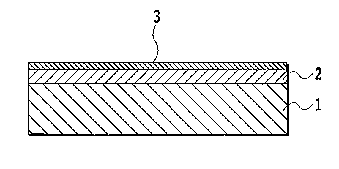
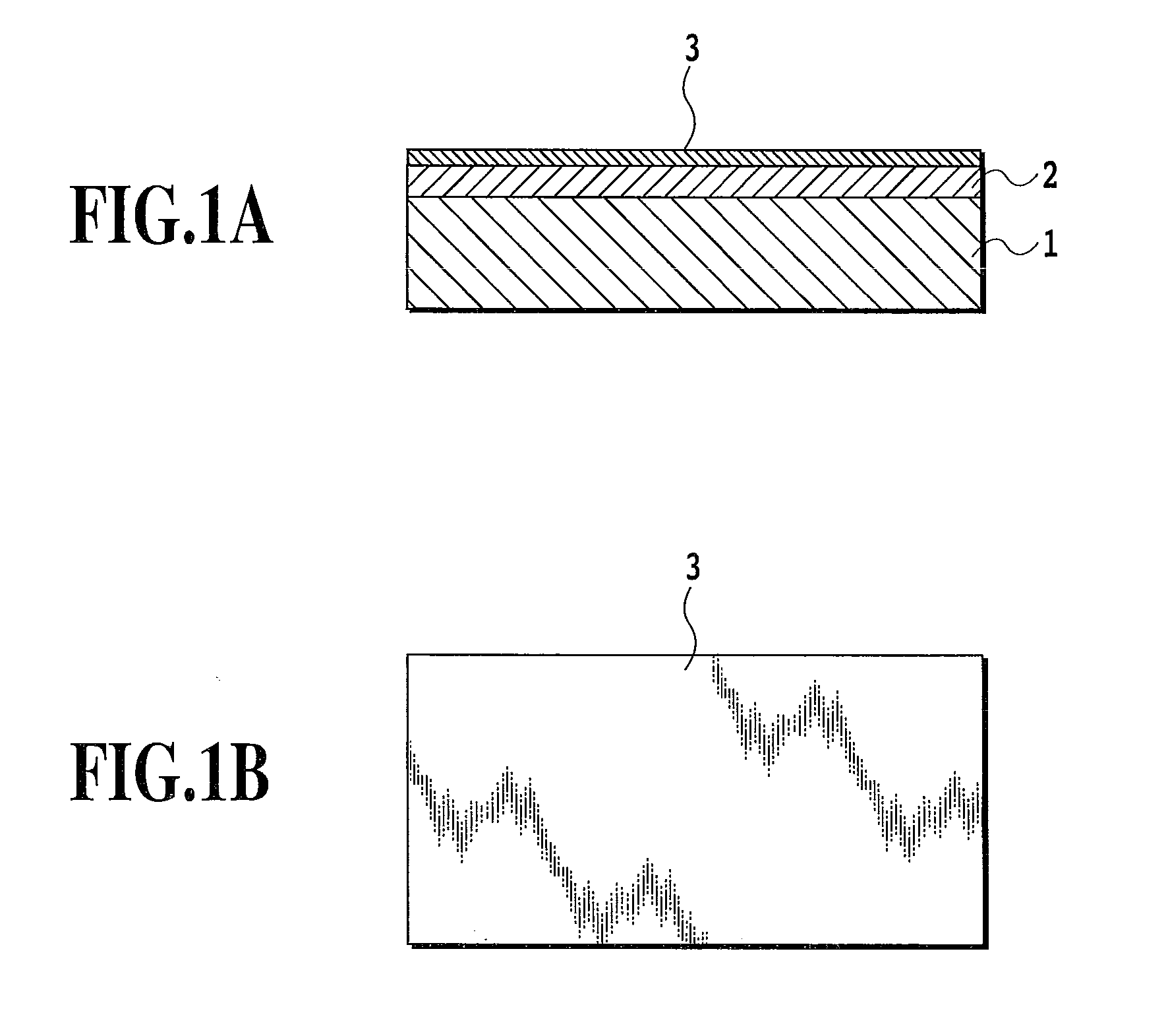
[0063]FIG. 1A and FIG. 1B are views showing a sectional structure of a thin film lamination in accordance with the present invention, a structural view showing an InAsSb thin film lamination in accordance with the present invention: FIG. 1A is a sectional view; and FIG. 1B is its top view. In these figures, the reference numeral 1 designates a substrate, 2 designates an AlxGayIn1-x-ySb mixed crystal layer (buffer layer) (0xSb1-x (0xSb1-x (0

[0064]In the thin film lamination in accordance with the present invention, the AlxGayIn1-x-ySb mixed crystal layer (02 whose lattice constant is equal or close to that of the InAsxSb1-x thin film conducting layer is formed on the substrate 1, and the InAsxSb1-x thin film conducting layer 3 is formed directly on the AlxGayIn1-x-ySb mixed crystal layer as the operating layer. By forming such an insulating AlxGayIn1-x-ySb mixed crystal layer (02 between the ...

example 2

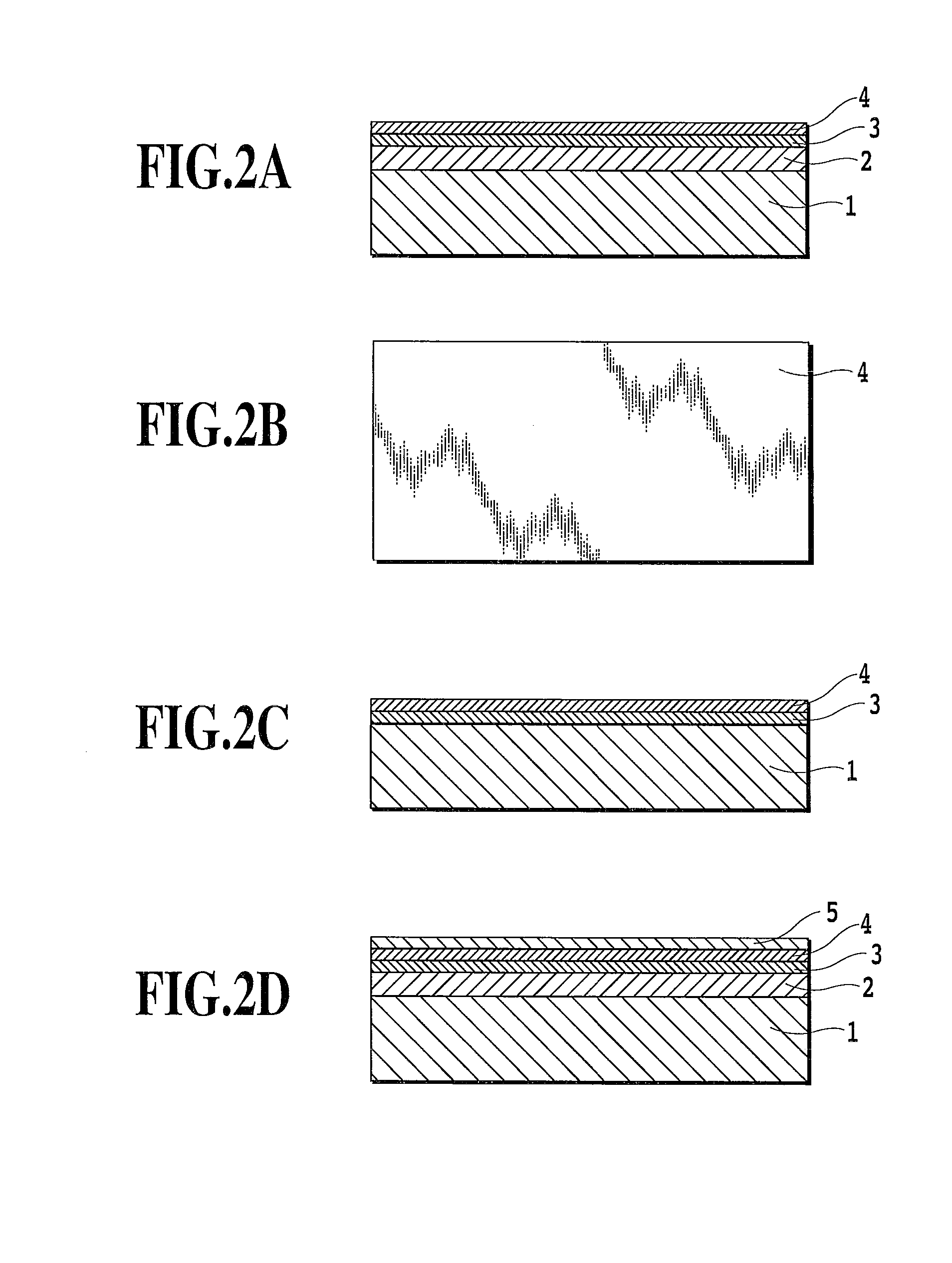
[0065]FIG. 2A to FIG. 2D are structural views of a thin film lamination in accordance with the present invention with a structure having an InAsSb thin film conducting layer constituting the operating layer sandwiched between an AlInSb mixed crystal layer 2 and an AlInSb mixed crystal layer 4 constituting a cap layer at its top and bottom: FIG. 2A is a sectional view; FIG. 2B is its top view; FIG. 2C is a sectional view of the thin film lamination when the InAsSb layer 3 constituting the operating layer is formed directly on a substrate 1, and the AlInSb mixed crystal layer 4 constituting an insulating layer of a cap layer is formed thereon; and FIG. 2D is a sectional view when a GaAs insulating protective layer 5 is formed.

[0066]The reference numeral 4 in FIG. 2A designates an AlInSb mixed crystal layer appearing on the top surface. A reason for assuming such a stacked structure is that since the electron mobility in the operating layer can be reduced because of a low electron mobi...

example 3

[0078]FIG. 3A and FIG. 3B are sectional views showing an example of a magneto-resistance element using a thin film lamination in accordance with the present invention. In FIG. 3A, the reference numeral 6 designates terminal electrodes for connecting the magneto-resistance element to the outside. The example has 3-layer metal thin film electrodes formed on the InAsSb operating layer 3 in ohmic contact. In addition, the reference numeral 7 designates 2-layer metal electrodes which are inserted between the terminal electrodes and are formed on the InAsSb thin film operating layer in ohmic contact. The electrodes 7, which are also called short-circuit electrodes or short-bar electrodes, are formed plurally between the terminal electrodes, and are used to improve the sensitivity of the magnetic resistance effect. FIG. 3B is a top view of the magneto-resistance element. The portion designated by the reference numeral 8 is a sensor section for detecting magnetism of the magneto-resistance ...


PUM

PropertyMeasurementUnit
thicknessaaaaaaaaaa
thicknessaaaaaaaaaa
thickaaaaaaaaaa

Abstract

Relating to a thin film lamination and a thin film magnetic sensor using the thin film lamination and a method for manufacturing the thin film lamination that realizes a thin film conducting layer having high electron mobility and sheet resistance as an InAsSb operating layer. A thin film lamination is provided which is characterized by having an AlxIn1-xSb mixed crystal layer formed on a substrate, and an InAsxSb1-x (0<x≦1) thin film conducting layer directly formed on the AlxIn1-xSb layer, in which the AlxIn1-xSb mixed crystal layer is a layer that exhibits higher resistance than the InAsxSb1-x thin film conducting layer or exhibits insulation or p-type conductivity, and its band gap is greater than the InAsxSb1-x thin film conducting layer, and the a lattice mismatch is +1.3% to −0.8%.

Description

TECHNICAL FIELD[0001]The present invention relates to a thin film lamination, a thin film magnetic sensor using the thin film lamination and a method for manufacturing the thin film lamination, and particularly to a thin film lamination, a thin film magnetic sensor using the thin film lamination and a method for manufacturing the thin film lamination applicable to semiconductor thin film magnetic sensors and the like.BACKGROUND ART[0002]An InSb single crystal thin film grown by a conventional MBE method has large electron mobility and is suitable as a material of Hall elements or magneto-resistance elements. For example, it is reported that a 1.0 μm thick InSb thin film formed on a semiconductor GaAs substrate by doping a proper quantity of Sn has small temperature dependence of resistance and exhibits very high electron mobility, and hence it is a material capable of realizing highly sensitive magnetic sensors such as magneto-resistance elements or Hall elements operating in a wide...

Claims


Application Information

Patent Timeline
Patent Type & Authority Applications(United States)
IPC IPC(8): G01R33/02B32B15/01H01L21/20H01L21/30
CPCG01R33/07H01L29/201H01L43/065H01L43/08H01L43/10H01L43/12Y10T428/12681H01L21/02395H01L21/02463H01L21/02466H01L21/02546H01L21/02549H01L21/0262H01L43/14H10N52/101H10N52/01H10N50/10H10N50/01H10N50/85G01R33/09H10N52/00
Inventor SHIBASAKI, ICHIROGEKA, HIROTAKAOKAMOTO, ATSUSHI
Owner ASAHI KASEI KK
Why Eureka
Try Eureka