
Semiconductor device and method of manufacturing the same

a technology of semiconductors and semiconductors, applied in the field of semiconductor devices, can solve the problems of low conduction controllability, chemical instability of swnts channels, and inability to manufacture stably operable devices, etc., and achieve the effects of low power consumption of el elements, low cost, and simple structure of el elements

Inactive Publication Date: 2010-03-04
NEC CORP
View PDF1 Cites 20 Cited by
  • Summary
  • Abstract
  • Description
  • Claims
  • Application Information

AI Technical Summary

Benefits of technology

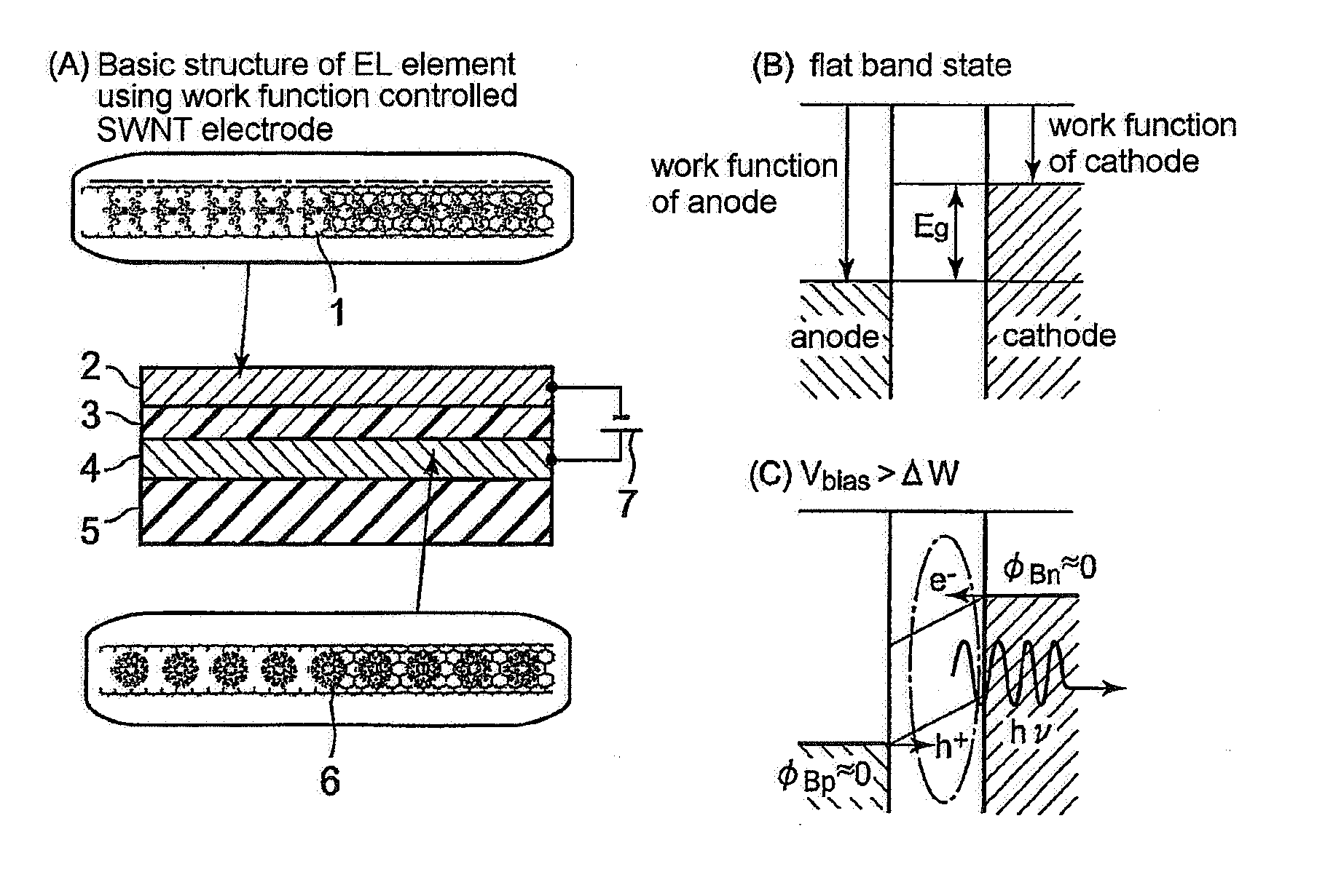
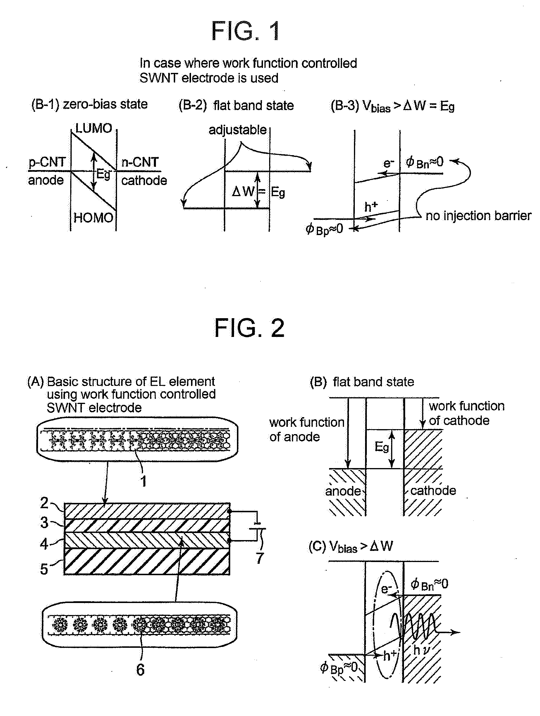
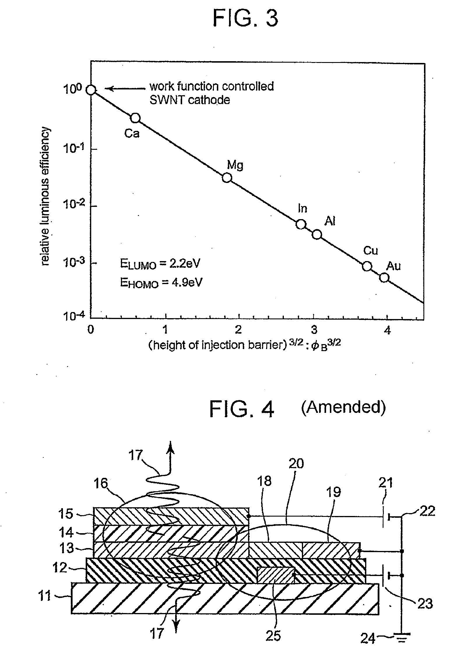
[0035]In the semiconductor device according to the present invention, it is possible to contribute to low power consumption of the EL element because a limiting factor in injection at an electrode interface of the element is reduced or suppressed by using SWNTs electrode whose work function is controlled by encapsulation. Further, in the semiconductor device of the present invention, it is possible to contribute to simplification in structure of the EL element and to small size and light weight of an array and a display device constructed by the EL elements because an electrode and an injection layer are integrated in an encapsulating SWNTs electrode. Therefore, with the semiconductor device and the method of manufacturing the same according to the present invention, characteristics and performance of the EL element can be improved.
[0036]Further, with the semiconductor device and the method of manufacturing the same according to the present invention, use of the encapsulating SWNTs electrode eliminates an injection barrier at the interface between the electrode and the light-emitting layer and prevents reaction and migration between the electrode and the light-emitting layer. Therefore, it is possible to prevent the problem of degradation of the electrode and the light-emitting layer, such as a dark spot specific to the EL element, and to contribute to an increase in life of the element. Thus, improvement in reliability of the EL element can be achieved.
[0037]Furthermore, with the semiconductor device and the method of manufacturing the same according to the present invention, the encapsulating SWNTs electrode can be manufactured by an atmospheric room-temperature process. Therefore, a manufacturing process of the EL element is simplified and a manufacturing cost can drastically be reduced. Thus, improvement in productivity of the EL element can be achieved.

Problems solved by technology

However, SWNTs channels formed by both of the above-mentioned methods are not suitable for fabrication of a device that is stably operable.
This is because the SWNTs channel is chemically unstable in the atmosphere since the donor exists outside SWNTs walls.
The n-type conduction SWNTs produced by those methods are stable in the atmosphere but are low in conduction controllability, such as a carrier density, because of use of an organic material.
Therefore, it is not possible to manufacture a reliable device.
This results in flowing of useless current which does not contribute to light emission without occurrence of recombination.

Method used


Image

  • Semiconductor device and method of manufacturing the same
  • Semiconductor device and method of manufacturing the same
  • Semiconductor device and method of manufacturing the same

Examples


examples

[0072]Next, examples of the present invention will be described. However, the present invention is not limited to these examples.

first example

[0073]Work function controllability of the SWNTs material shown in the present invention was examined both experimentally and theoretically. First, a SWNTs transistor having SWNTs as a channel was formed by a method described in Patent Document 4 (JP-A-2004-67413). Briefly describing the SWNTs transistor, gold / titanium was used for source and drain electrodes, a silicon oxide film of about 100 nm was used for an insulating layer, and highly-doped n-type silicon / gold was used for a gate electrode. The SWNTs channel was formed by in-situ growth by the catalytic chemical vapor deposition using hydrocarbon, such as methane, as a source material. The SWNTs channel has a diameter of typically 1 to 2 nm and a length of about 300 nm which is defined by a distance between the source electrode and the drain electrode. Next, the SWNTs channel was doped with a donor, such as cesium (IP=3.89 eV), potassium (IP=4.34 eV), or indium (IP=5.79 eV) by ion beam deposition and a drain current-gate volta...

second example

[0077]By the technique same as the first example, work function controllability of an acceptor doped SWNTs was examined. FIG. 7 shows an acceptor surface density dependence of work function shift of the acceptor doped SWNTs. (A) shows a case of fullerene monofluoride: C60F (EA=2.78 eV), (B) shows a case of iodine (EA=3.08 eV), and (C) shows a case of tantalum fluoride: TaF6 (EA=8.4 eV). Contrary to the donor doped SWNTs, as the acceptor surface density is increased, the work function shift is drastically extended in a plus direction so that the work function of the SWNTs is increased. When the acceptor surface density is around 1×1013 cm−2 in the cases of (A) and (B) and when the acceptor surface density is around 5×1013 cm−2 in the case of (C), the work function shifts tend to be saturated. At the acceptor surface density around 1×1015 cm−2, the work function shift is plus 0.6 eV in the cases of (A) and (B) and plus 0.68 eV in the case of (C) by actual measurement.

[0078]The accepto...


PUM

PropertyMeasurementUnit
ionization potentialaaaaaaaaaa
temperatureaaaaaaaaaa

Abstract

A semiconductor device has a structure in which a light-emitting layer of an organic material or the like is sandwiched between a work function controlled single-wall carbon nanotube cathode encapsulating a donor having a low ionization potential and a work function controlled single-wall carbon nanotube anode encapsulating an acceptor having a high electron affinity. A semiconductor device represented by an organic field-effect light-emitting element and a method of manufacturing the same are provided. The semiconductor device and the method of manufacturing the same make it possible to improve characteristics and performance, such as reduction in light-emission starting voltage and a high luminous efficiency, to improve reliability, such as an increase in life, and to improve productivity, such as reduction in manufacturing cost.

Description

TECHNICAL FIELD[0001]This invention relates to a semiconductor device and a method of manufacturing the same and, in particular, to a field-effect self-luminous semiconductor device which is stable, high in injection efficiency, and low in power consumption and a method of manufacturing the same.BACKGROUND ART[0002]At first, description will be made about an organic electroluminescence (ElectroLuminescence: EL) element and single-wall carbon nanotubes (Single-Wall carbon NanoTubes: abbreviated to SWNTs) material, both of which are related to this invention.[0003]First, the organic EL element is a kind of light-emitting diode driven by a direct current and is also called an organic electroluminescence element and an organic LED (Light-Emitting Diode). At any rate, the most basic structure of the organic EL element mostly is a sandwich structure such that a light-emitting layer (might be called a luminescent layer) formed of an organic compound is sandwiched by two electrodes, i.e., a...

Claims


Application Information

Patent Timeline
Patent Type & Authority Applications(United States)
IPC IPC(8): H01L51/52H01L33/00H01L51/56
CPCB82Y10/00H01L51/0048H01L51/444H01L51/5203Y10S977/735Y10S977/75Y10S977/84Y10S977/949Y02E10/549Y02P70/50H10K85/221H10K30/821H10K50/805
Inventor HIURA, HIDEFUMITOGUCHI, SATORUTADA, TETSUYAKANAYAMA, TOSHIHIKO
Owner NEC CORP
Learn More