Al alloy film for display device,display device, and sputtering target

a technology of display device and sputtering target, which is applied in the direction of conductors, semiconductor/solid-state device details, instruments, etc., can solve the problems of reducing the display quality of the screen, the inability to carry out electric ohmic coupling, and the inability to directly connect the wire to the transparent pixel electrode. , to achieve the effect of excellent dry etching property, high performance and excellent productivity

Active Publication Date: 2010-03-18
KOBE STEEL LTD
View PDF3 Cites 29 Cited by
  • Summary
  • Abstract
  • Description
  • Claims
  • Application Information

AI Technical Summary

Benefits of technology

[0053]Further, by controlling the content of Gd and/or La, it is possible to have excellent dry etching property in addition to the foregoing property.
[0054]Use of the...

Problems solved by technology

When the Al type thin film is directly connected to the transparent pixel electrode 5, the coupling resistance (contact resistance) increases, resulting in degradation of the display quality of the screen.
Namely, Al forming the wire to be directly connected to the transparent pixel electrode is very susceptible to oxidation.
However, electric ohmic coupling cannot be carried out due to the Al oxide layer formed in the foregoing manner.
With the advance of reduction of cost with the trend for the mass production of liquid crystal displays, the increase in manufacturing cost and the reduction of the productivity entailed by formation of the barrier metal layer have become impossible to disregard.
However, with this...

Method used


Image

  • Al alloy film for display device,display device, and sputtering target
  • Al alloy film for display device,display device, and sputtering target
  • Al alloy film for display device,display device, and sputtering target

Examples


embodiment 1

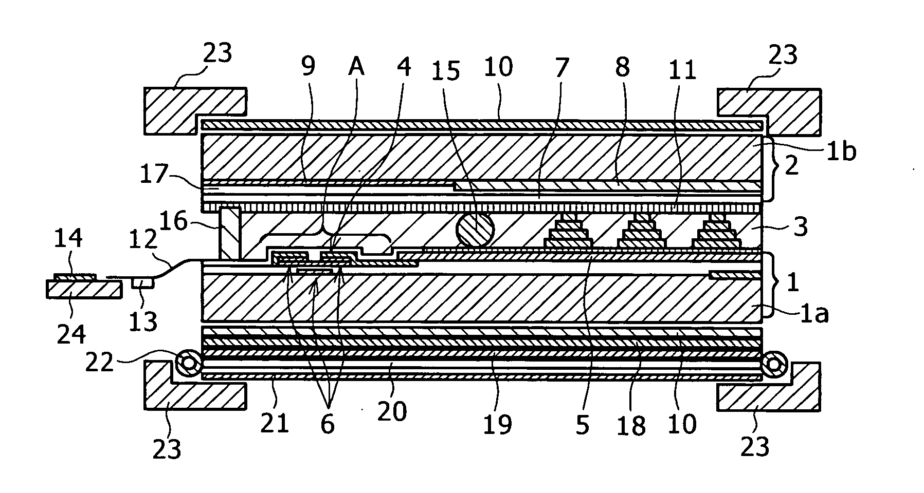
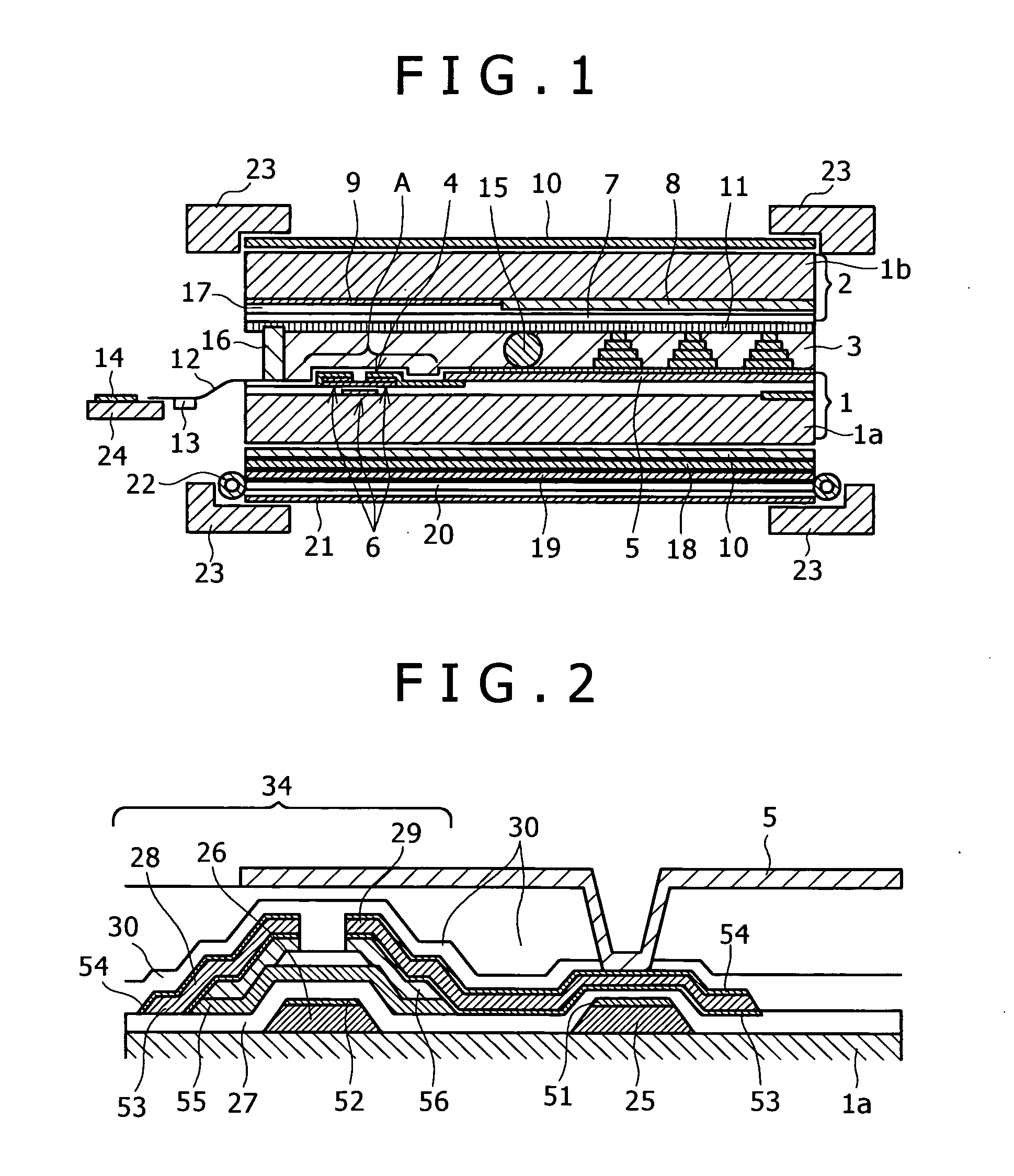
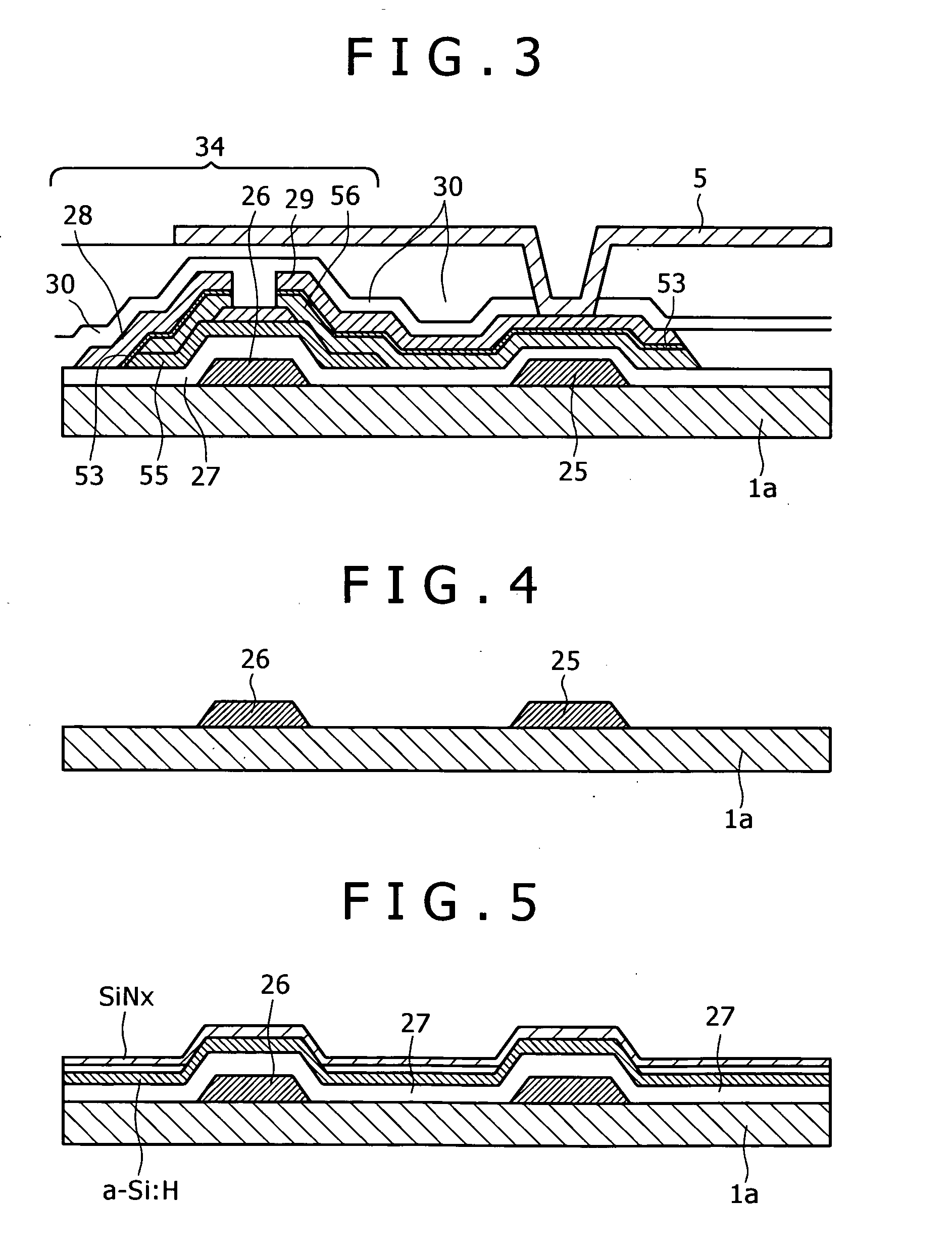
[0157]By reference to FIG. 3, an embodiment of an amorphous silicon TFT substrate will be described in details. FIG. 3 is a schematic cross sectional illustrative view for illustrating a preferred embodiment of a bottom gate type TFT substrate in accordance with the present invention. In FIG. 3, the same reference numerals as those in FIG. 2 described above, indicating a conventional TFT substrate are given.

[0158]Apparent from the comparison between FIG. 2 and FIG. 3, in the conventional TFT substrate, as shown in FIG. 2, on a scanning line 25, on a gate electrode 26, and on or under a source-drain wire 34, barrier metal layers 51, 52, 54, and 53 are formed, respectively. In contrast, in the TFT substrate of this embodiment, the barrier metal layers 51, 52, and 54 can be omitted. Namely, in accordance with this embodiment, the wiring material for use in a source-drain electrode 29 of the TFT can be directly connected to a transparent pixel electrode 5 without allowing a barrier meta...

embodiment 2

[0175]With reference to FIG. 12, an embodiment of the polysilicon TFT substrate will be described in details.

[0176]FIG. 12 is a schematic cross sectional illustrative view for illustrating a preferred embodiment of a top gate type TFT substrate in accordance with the present invention. In FIG. 12, the same reference numerals as those in FIG. 2 described above, indicating a conventional TFT substrate are given.

[0177]This embodiment is mainly different from Embodiment described above in that polysilicon is used in place of amorphous silicon as the active semiconductor layer, in that a TFT substrate of not a bottom gate type but a top gate type is used, and in that the Al-0.2 at % Ge-0.2 at % Gd alloy satisfying the requirements of the present invention is used not as the wiring material for the source-drain electrodes and the gate electrodes, but as the wiring material for the source-drain electrodes. Minutely, the polysilicon TFT substrate of this embodiment shown in FIG. 12 is diffe...

experimental example 1

[0211]As the Al alloy films, 5 kinds of samples of Al-0.3 at % α-0.35 Gd at % (α=Ni, Ge, Ag, Zn, and Cu) were prepared. Each of them was measured for the contact resistivity with the ITO film. The measurement method of the contact resistance was as follows. A Kelvin pattern (contact hole size: 10 μm square) shown in FIG. 20 was manufactured, and the four-terminal measurement (a method in which an electric current is caused to flow through the ITO-Al alloy or the IZO-Al alloy, and at another terminal, the voltage drop across the ITO-Al alloy or the IZO-Al alloy is measured) was performed. Specifically, a current I is caused to flow across I1-I2 of FIG. 20, and the voltage V across V1-V2 was monitored, thereby to determine the contact resistance R of the contact part C as [R=(V1−V2) / I2].

[0212]FIG. 21 shows the results when ITO was used as the transparent pixel electrode. The same tendency as that in FIG. 21 was also observed when IZO was used in place of ITO. FIG. 21 indicates that th...


PUM

PropertyMeasurementUnit
Electrical resistivityaaaaaaaaaa
Volumeaaaaaaaaaa
Volumeaaaaaaaaaa

Abstract

The present invention provides an Al alloy film for a display device, to be directly connected to a conductive oxide film on a substrate, the Al alloy film comprising Ge in an amount of 0.05 to 0.5 at %, and comprising Gd and/or La in a total amount of 0.05 to 0.45 at %, a display device using the same, and a sputtering target for the display device. For the Al alloy film of the present invention, even when a barrier metal is not provided, and a conductive oxide film and the Al alloy film are directly connected, the adhesion between the conductive oxide film and the Al alloy film is high, and the contact resistivity is low, and preferably, the dry etching property is also excellent.

Description

TECHNICAL FIELD[0001]The present invention relates to an Al alloy film for a display device for use in a liquid crystal display, a semiconductor, an optical component, or the like, a display device, and a sputtering target for a display device. More particularly, it relates to a novel wiring material including an Al alloy film as a constituent element.BACKGROUND ART[0002]Liquid display devices for use in various fields from compact cellular phones to more than 30-inch large-size televisions are classified into simple matrix type liquid crystal display devices and active matrix type liquid crystal display devices according to the driving method of pixels. Out of these, an active matrix type liquid crystal display device having a thin film transistor (which is hereinafter referred to as a TFT) as a switching element can implement a high precision image quality; and is adaptable to high-speed images or the like, and hence it has been used for general purposes.[0003]With reference to FI...

Claims


Application Information

Patent Timeline
IPC IPC(8): H01L33/00H01B5/00C23C14/34
CPCH01L23/53219H01L29/458H01L29/4908H01L27/124H01L2924/0002H01L2924/00G02F1/136286
Inventor GOTOU, HIROSHITOMIHISA, KATSUFUMIHINO, AYAOKUNO, HIROYUKINAKAI, JUNICHIKAWAKAMI, NOBUYUKIOCHI, MOTOTAKA
Owner KOBE STEEL LTD
Why Eureka
Try Eureka