
Method for forming metal film by ald using beta-diketone metal complex

a metal complex and metal film technology, applied in the direction of resistive material coating, liquid/solution decomposition chemical coating, superimposed coating process, etc., can solve the problems of difficult to form good wirings, discontinuous cu films formed by pvd method on top of these barrier films, and difficult to form barrier films having a uniform thickness. , to achieve the effect of low resistance, high shielding property and easy adsorption on the substra

Active Publication Date: 2010-04-15
ASM JAPAN
View PDF36 Cites 333 Cited by
  • Summary
  • Abstract
  • Description
  • Claims
  • Application Information

AI Technical Summary

Benefits of technology

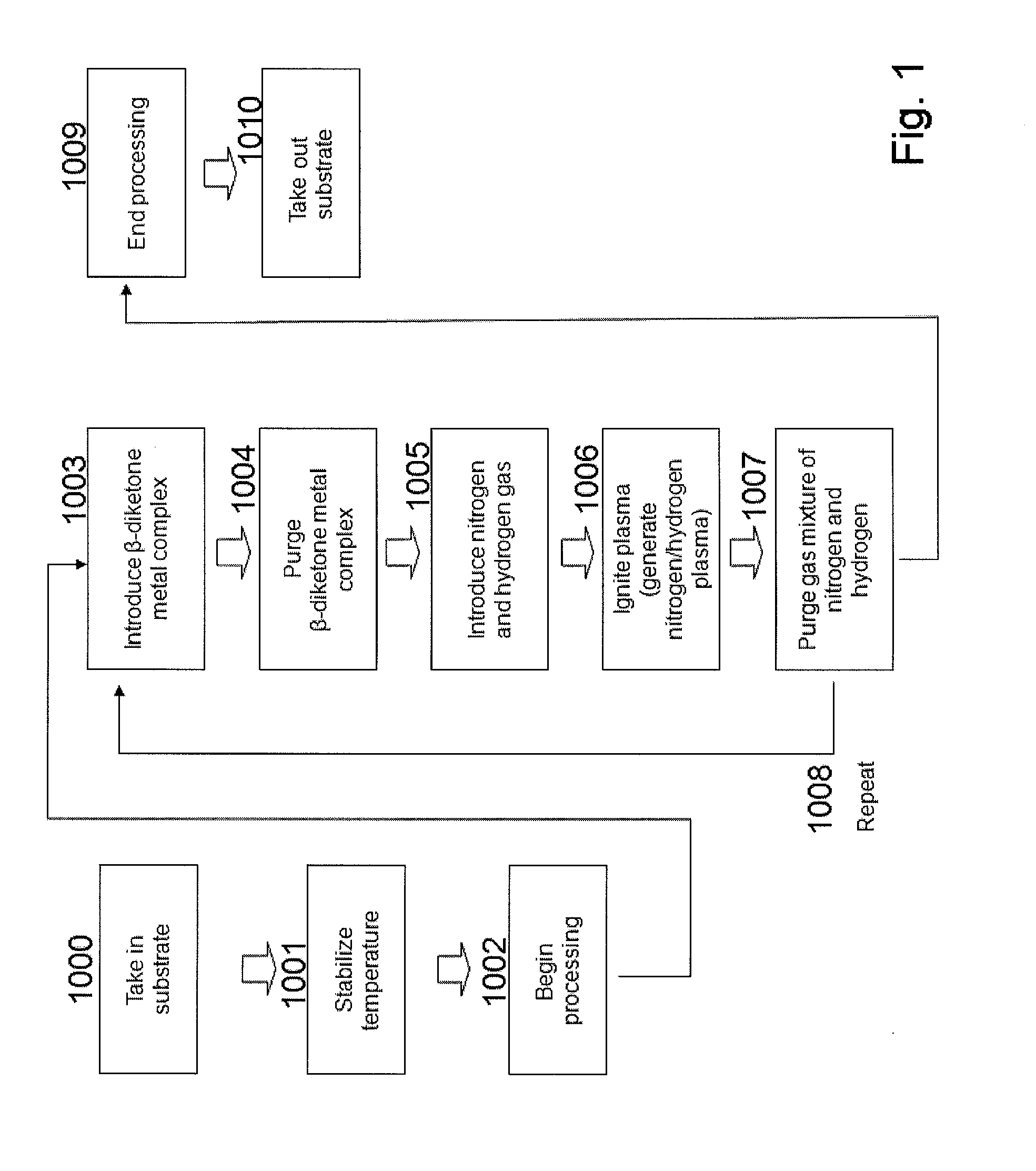
[0008]An embodiment of the present invention provides a method for forming a film at low temperature and in a reducing atmosphere from a material that constitutes a metal element where β-diketone can be coordinated, such as any one of 8B, 1B and 2B family elements, or specifically Fe, Ni, Rh, Pd, Ir, Pt, Co, Ru and Cu in practical settings, wherein the resulting metal film exhibits low resistivity and high shielding property. The basic principles of the present invention are achieved by two processes. When any of the aforementioned metal complexes coordinated by β-diketone (hereinafter referred to as “β-diketone metal complexes”) is supplied to a substrate, such β-diketone metal complex has the property of easily adsorbing onto the substrate. Accordingly, the first principle of the present invention is that the β-diketone metal complex can be easily adsorbed onto the substrate surface in a uniform manner regardless of whether a metal film or oxide film is formed. The second principle is that by exposing the metal complex coordinated by β-diketone to a mixture gas of hydrogen and nitrogen that has been activated by plasma, β-diketone groups can be eliminated from the metal element in an extremely quick and reliable manner. By allowing the metal atoms to remain on the substrate surface this way, a metal film can be formed with ease. This quick and reliable elimination of β-diketone groups from the metal element dramatically increases the atomic layer deposition rate and also dramatically improves the purity of the metal element in the formed atomic layer.

Problems solved by technology

With the PVD method, however, it is difficult to form barrier films having a uniform thickness over wirings of high aspect ratios or via holes and contact holes used for connecting wirings, and instead the PVD method tends to produce discontinuous films on side faces of trenches, via holes and contact holes, especially on side faces at the bottom of height gaps, as the film thickness decreases.
As a result, Cu films formed by the PVD method on top of these barrier films also tend to become discontinuous.
For this reason, voids generate in electroplated copper layers where these discontinuous Cu films are used as seeds, which makes it difficult to form good wirings.
In the case of the CVD method, high impurities and consequent low surface smoothness make it generally difficult to form a continuous film when the film thickness is reduced.
Furthermore, it is difficult to achieve good adhesion when a Cu film is formed on top of the aforementioned film lacking in continuity.
Although the CVD method normally achieves good shielding property under general conditions, when finer elements are needed and thus the aspect ratios of wiring trenches and connection holes must be increased substantially, it is difficult to shield the wirings effectively.
With this method, however, finding a proper combination of a type of molecule that can be adsorbed to achieve good shielding property on one hand, and a type of reactant gas capable of easily breaking down the ligands of such molecule on the other, is difficult, and normally the resulting film tends to contain impurities such as residual carbon, oxygen and nitrogen and its resistivity is also likely much higher than the intended level.
Under this method, however, the formed Co film tends to contain residual carbon and oxygen from the organic metal material and it is therefore difficult to obtain a quality Co film offering low resistivity.
When oxygen gas was supplied, the problem of oxidization of the TaN film at the foundation occurred.

Method used


Image

  • Method for forming metal film by ald using beta-diketone metal complex
  • Method for forming metal film by ald using beta-diketone metal complex
  • Method for forming metal film by ald using beta-diketone metal complex

Examples


example 1

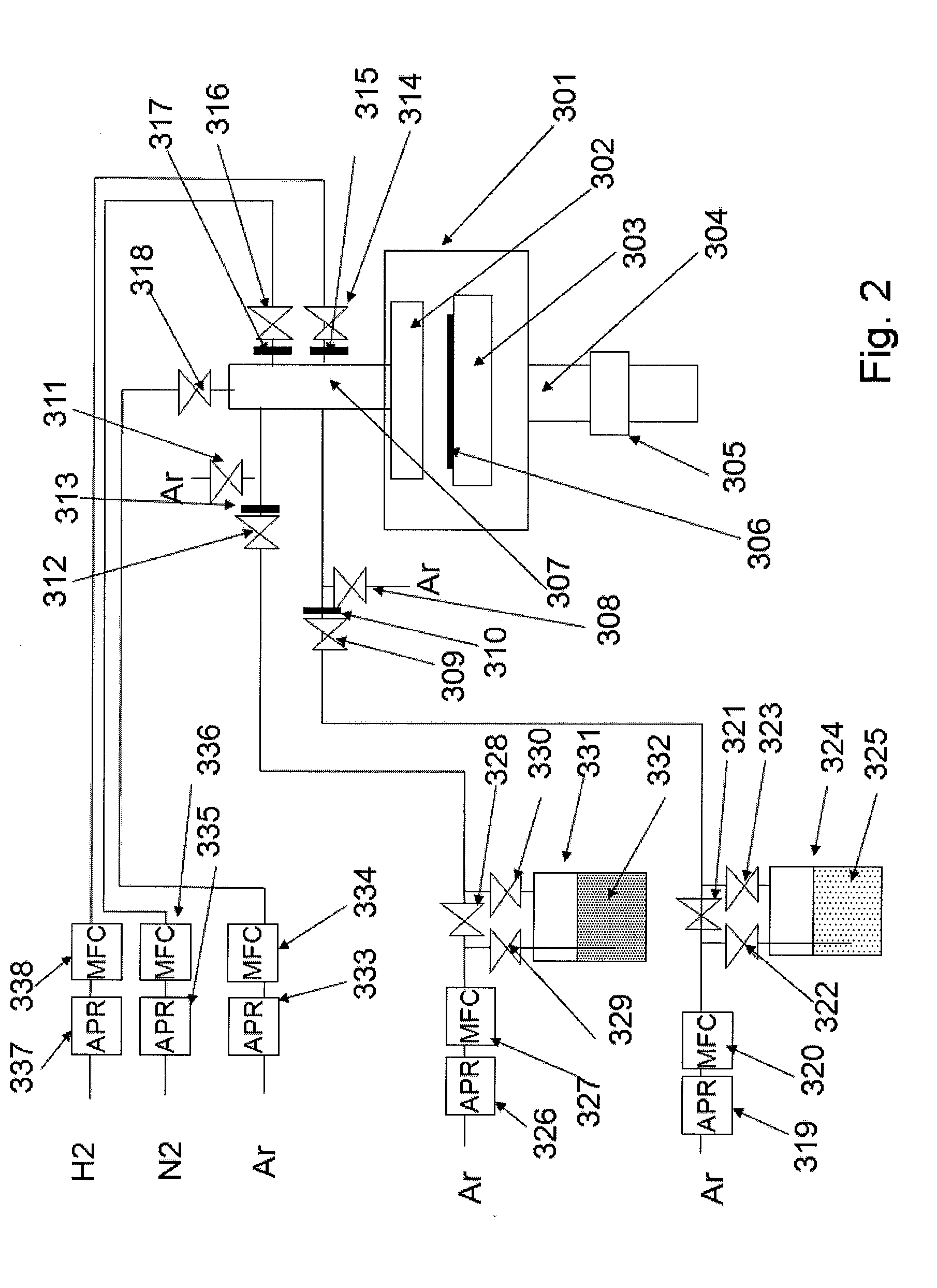
[0173]In this example, a process of forming a Co film is illustrated. Using the ALD apparatus shown in FIG. 2, an inter-layer connection structure using a Co film was formed according to the steps shown in FIGS. 3A to 3F.

[0174]In FIG. 2, the heating base 303 in the processing chamber 301 was set to 300° C. The Co material 325, or tridipivaloylmathanatocobalt (DPM3CO), was filled in a bottle 324 and this bottle was heated to 120° C. This Co material 325 had a vapor pressure of 0.5 torr, and vapor of the Co material was supplied by an argon carrier gas to a substrate via a valve 309 and orifice 310. After the Co material was supplied for 1 to 3 seconds, or desirably 1 second, this Co material was purged by the argon gas supplied from a valve 318, after which N2 was supplied by 50 sccm from a valve 316 and orifice 317, followed by the supply of H2 by 200 sccm from a valve 314 and orifice 315. High frequency power of 200 to 500 W and 13.56 MHz was then applied to this mixture gas and th...

example 2

[0177]In this example, an inter-layer connection structure was formed through the procedure shown in FIGS. 5A to 5F using a process of forming Ru and Cu films continuously in the same reaction chamber. In the ALD apparatus shown in FIG. 2, one material 325 is a Ru material containing β-diketone ligands, while the other material 332 is a Cu material containing β-diketone ligands.

[0178]A substrate was transferred to the reaction chamber, and first in FIG. 2 the heating base 303 in the processing chamber 301 was set to 300° C. The Ru material, or tridipivaloylmathanatoruthenium (DPM3Ru) 325, was filled in a bottle 324, and this bottle was heated to 120° C. This Ru material 325 had a vapor pressure of 0.1 torr, and vapor of the Ru material was supplied by an argon carrier gas to the substrate via a valve 309 and orifice 310. After the Ru material was supplied for 5 to 10 seconds, or desirably 5 seconds, this Ru material was purged by the argon gas supplied from a valve 318, after which ...

example 3

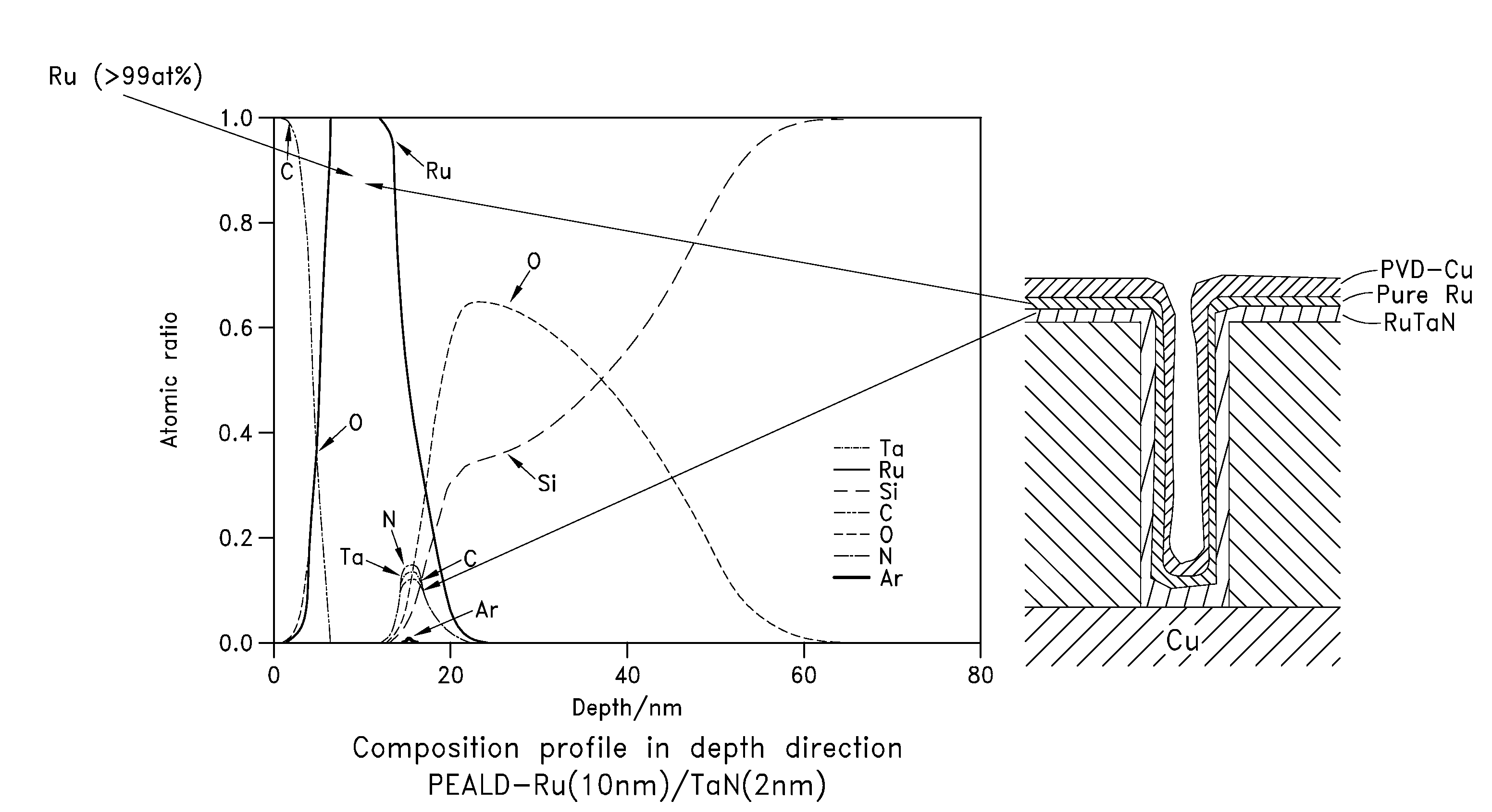
[0183]This example illustrates a process of forming a RuTaN film as a Cu barrier layer and then forming Ru and Cu layers. In the ALD apparatus shown in FIG. 2, one material 325 is a Ru material containing β-diketone ligands, while the other material 332 is a Ta organic metal material.

[0184]A substrate was transferred to the reaction chamber, and first in FIG. 2 the heating base 303 in the processing chamber 301 was set to 300° C. The Ta material, or TAIMATA (tertiaryamylimidotris(dimethylamido)tantalum), was supplied for 1 second. Taimata was supplied by an Ar carrier gas from a bottle 331 heated to 80° C. Next, 50 sccm of N2 was supplied from a valve 316 and orifice 317, and 200 sccm of H2 was supplied from a valve 314 and orifice 315. High frequency power of 200 to 500 W and 13.56 MHz was then applied to this mixture gas and the excited plasma was used to break down the Taimata adsorbed onto the substrate into Ta atoms. Although the plasma application time varies depending on the ...


PUM

PropertyMeasurementUnit
Temperatureaaaaaaaaaa
Thicknessaaaaaaaaaa
Fractionaaaaaaaaaa

Abstract

A method of forming a single-metal film on a substrate by plasma ALD includes: contacting a surface of a substrate with a β-diketone metal complex in a gas phase; exposing molecule-attached surface to a nitrogen-hydrogen mixed plasma; and repeating the above steps, thereby accumulating atomic layers to form a single-metal film on the substrate.

Description

BACKGROUND OF THE INVENTION[0001]1. Field of the Invention[0002]The present invention, generally, relates to a method for forming metal wirings that can be used favorably in the creation of fine semiconductor elements. More specifically, the present invention relates to a method for forming a metal film by atomic layer deposition using a β-diketone metal complex.[0003]2. Description of the Related Art[0004]Next-generation fine semiconductor elements require formation of semiconductor elements having not only two-dimensional structures, but also three-dimensional structures. Accordingly, the formation of metal wirings for such fine semiconductor elements also requires the ratio of wiring height to wiring width to be improved to a range of 5 to 10, and the ratio of height to hole diameter to a range of approx. 5 to 10 for connection holes used to connect top-layer wirings and bottom-layer wirings. For this reason, it becomes necessary, when forming copper wirings for use as these meta...

Claims


Application Information

Patent Timeline
IPC IPC(8): B05D3/14
CPCC23C16/18C23C16/45542C23C16/45531
Inventor SHINRIKI, HIROSHINAMBA, KUNITOSHIJEONG, DAEKYUN
Owner ASM JAPAN
Learn More