
Microwave activation annealing process

a technology of activation and annealing process, which is applied in the direction of semiconductor devices, electrical apparatus, transistors, etc., can solve the problems of degrading process efficiency, limiting the duration of the work object on the high temperature generated in the activation procedure of the process, and generating thermal destruction on the object to be manufactured, etc., to achieve high electron mobility, provide energy in a very quick way, and high efficiency

Inactive Publication Date: 2010-05-13
NAT APPLIED RES LAB
View PDF4 Cites 29 Cited by
  • Summary
  • Abstract
  • Description
  • Claims
  • Application Information

AI Technical Summary

Benefits of technology

[0014]The main objective of the present invention is to provide a microwave activation annealing process which not only won't destruct the material property and the structural interface, but also can shorten process time and enhance heating homogeneity.
[0021]Through the above mentioned method, the activation annealing process of the present invention of microwave activation annealing process, because the energy provided by the microwave can only be absorbed by the semiconductor device, the doped atom in the material of the object to be manufactured will rotate instead of vibrate so as to complete the bond repair; moreover, the air in the device and the corresponding container all will not generate heat, hence, the efficiency is very high; in addition, since the microwave can provide energy in a very quick way, temperature is very low and heating is very homogeneous, hence, it can improve the time-consuming, high temperature and bad homogeneity drawbacks generated in the commonly used thermal treatment techniques of high tech industries such as semiconductor packaging, optoelectronic and solar cell, etc.

Problems solved by technology

To the glass substrate and the soft flexible substrate, through the heating method, the Amorphous Silicon Layer is converted to Polysilicon or even Single Crystal Silicon so as to enhance the device characteristic of the semiconductor device; however, the glass substrate and the soft flexible substrate can not resist the high temperature process, hence, the activation process is changed to laser heating treatment.
However, under the current trend of small form factor and miniaturization for the high tech electronic product, the dimension of work object to be manufactured thus gradually diminish in its dimension, hence, the endurance of the work object on the high temperature generated in the activation procedure of the process is then limited and it thus leads to the drawbacks of the generation of thermal destruction on the object to be manufactured.
For example, the heat treatment process of furnace will generate high temperature which will destruct the material property, destruct the structural interface, result in junction diffusion and inter-diffusion, etc.
; in addition, the longer process time needed by the furnace also makes some degrade on the process efficiency.
Furthermore, although the heat treatment process of RTA is very short, yet its high temperature still causes the drawbacks such as: damage of material the characteristics, damage of the structural interface and the inter-diffusion.
In addition, let's take the LASER heat treatment process as an example, although it has lower heat treatment temperature and smaller thermal damage and has the advantage of partial treatment, yet the entire process time is lengthened and it is impossible to provide good heating homogeneity.
To sum up, we can see that currently, in the high tech electronic industry, no matter the substrate is made of what material, the currently used high temperature activation annealing thermal treatment techniques have the drawbacks such as high temperature thermal damage, longer process time or heating homogeneity, etc.

Method used


Image

  • Microwave activation annealing process
  • Microwave activation annealing process
  • Microwave activation annealing process

Examples


first embodiment

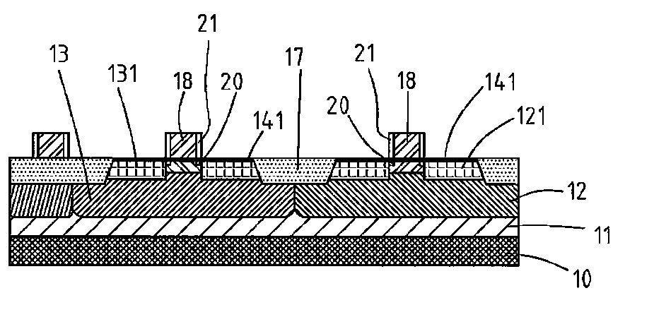
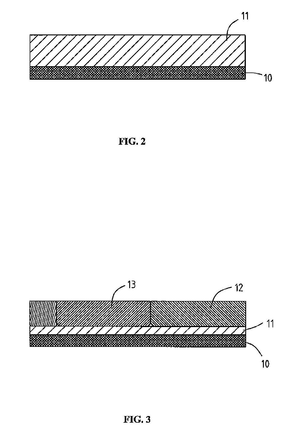
[0044]Please refer to FIG. 2 to FIG. 7, which is the present invention; in the embodiment, the microwave activation annealing process of the present invention is applied in Complementary Metal Oxide Semiconductor Field Effect Transistor process; as shown in FIG. 2, silicon-based substrate is supplied to be used as P type bare wafer (10) and the P type bare wafer (10) is cleaned, then epitaxy deposition is performed to form a P type epitaxial layer (11); as shown in FIG. 3, photo mask is used on the P type epitaxial layer (11) to perform microlithography process so as to form a N well (12); meanwhile, the N well (12) is implanted with P ion, and a photo mask is further used on the P type epitaxial layer (11) to perform microlithography process to form P type well (13), then the P type well (13) is implanted with boron ion, and finally the photo resist is stripped.

[0045]As shown in FIG. 4, above the N type well (12) and the P type well (13) is made with an pad oxide layer (14); meanwh...

second embodiment

[0051]Please refer to FIGS. 8 to 10, which is the present invention; in the embodiment, the microwave activation annealing process of the present invention is used in Metal Semiconductor Field Effect Transistor process; as shown in FIG. 8, a compound substrate of GaAs semi-insulating substrate (30) is supplied, epitaxial way is used to stack in sequence a buffer layer (31), a Schottky layer (32) and a cap layer (33); then dry etching method is used to do dicing and mesa isolation to form several mutually separated blocks.

[0052]As shown in FIG. 9, on the cap layer (33) of one of the blocks, the microlithography process is used to form metal contact between the source electrode (34) and the drain electrode (35); then the microwave activation annealing is performed with microwave activation frequency of 5.8 GHz and microwave activation temperature of 320° C., and the microwave annealing frequency can also be 5.8 GHz with microwave annealing temperature also 320° C., hence the contact r...

third embodiment

[0054]Please refer to FIG. 11 to FIG. 14, which is the present invention; in the embodiment, the microwave activation annealing process of the present invention is used in a Thin Film Transistor process; as shown in FIG. 11, a glass substrate (40) is supplied and glass inspection is done to inspect if there are any defects on the glass substrate (40); then chemical vapor deposition (CVD) is used to deposit a silicon dioxide buffer layer (41) and on the silicon dioxide buffer layer (41) is then deposited again with a hydrogenated amorphous silicon (a-Si:H)(42); then a dehydrogenation step is used to strip off the hydrogen in the hydrogenated amorphous silicon (42).

[0055]As shown in FIG. 12, then the next thing to do is crystallization, then the definition and etching of ploy-Si island (43) is done. As shown in FIG. 13, CVD is used to perform gate electrode dielectric layer deposition so as to form a gate dielectric layer (44) to cap poly-silicon island (43), then deposition and etchi...


PUM


Abstract

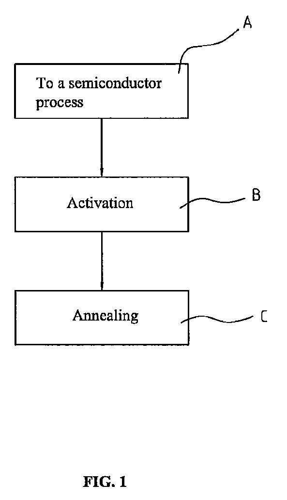
The present invention relates a microwave activation annealing process, which includes: the providing of a semiconductor process to form a semiconductor device on a substrate; activation: using a microwave device to perform microwave activation on the semiconductor device with frequency in the range of 2.45 GHz and 24.15 GHz and temperature in the range of 100° C. and 600° C.; annealing: using the microwave device to perform microwave annealing on the semiconductor device with frequency in the range 2.45 GHz to 24.15 GHz and temperature in the range 100° C. to 600° C.; by doing so, the present invention can, in the premise without the destruction of material property and structural interface and be able to shorten process time and enhance heating homogeneity, achieve the objective of activation annealing, hence, it can solve the defects caused by the heat treatment technique of prior art high temperature activation annealing.

Description

FIELD OF THE INVENTION[0001]The present invention relates to a microwave activation annealing process, it especially relates to a microwave activation annealing process that won't destruct the material property and the structural interface but can shorten the process time and enhance the heating homogeneity.BACKGROUND OF THE INVENTION[0002]In the high tech industries such as semiconductor packaging, optoelectronic and solar cell, etc., the work object must pass through the heat treatment process of one high temperature with subsequent low temperature cooling so that the work object can achieve the activation and the annealing purposes; currently, the commonly used heat treatment techniques include: high temperature furnace, LASER, Rapid Thermal Annealing (RTA), spike RTA, Flash Lamp Anneal, etc.[0003]Generally speaking, the above mentioned work objects include the following three categories:[0004]1. Si-Based Substrate, for example, Silicon Germanium, (SiGe), which can be used to man...

Claims


Application Information

Patent Timeline
Patent Type & Authority Applications(United States)
IPC IPC(8): H01L21/02
CPCH01L21/26513H01L21/324H01L29/201H01L21/2636H01L21/3245H01L29/6659H01L29/66742H01L29/66871H01L29/812H01L21/823814H01L21/823892H01L21/84H01L29/7833
Inventor HSUEH, FU-KUOLEE, YAO-JENWU, CHING-YI
Owner NAT APPLIED RES LAB
Learn More