Nitride semiconductor optical element and manufacturing method thereof

a manufacturing method and semiconductor technology, applied in semiconductor devices, lasers, semiconductor lasers, etc., can solve the problems of reduced laser lasing wavelength, reduced crystallinity, and increased production cost, and achieve the effect of improving crystallinity and reducing laser lasing wavelength

Active Publication Date: 2010-06-17
USHIO OPTO SEMICON
View PDF15 Cites 35 Cited by
  • Summary
  • Abstract
  • Description
  • Claims
  • Application Information

AI Technical Summary

Benefits of technology

[0009]In the conventional technique described in Patent Document 1, a method in which hydrogen is added to the interface between the well layer and the barrier layer at a rate of 0.01 to 1% is described, and it is reported that the segregation of In can be eliminated by the addition of hydrogen and the crystallinity is improved. However, there is a problem that, wh

Problems solved by technology

However, there is a problem that, when the growth interruption time after the well layer growth is long, the InN composition is desorbed from the surface of the InGaN well layer and the lasing wavelength of laser is reduced.
Moreover, there is also a problem that, since the effect of etching is increased when hydro

Method used


Image

  • Nitride semiconductor optical element and manufacturing method thereof
  • Nitride semiconductor optical element and manufacturing method thereof
  • Nitride semiconductor optical element and manufacturing method thereof

Examples


first embodiment

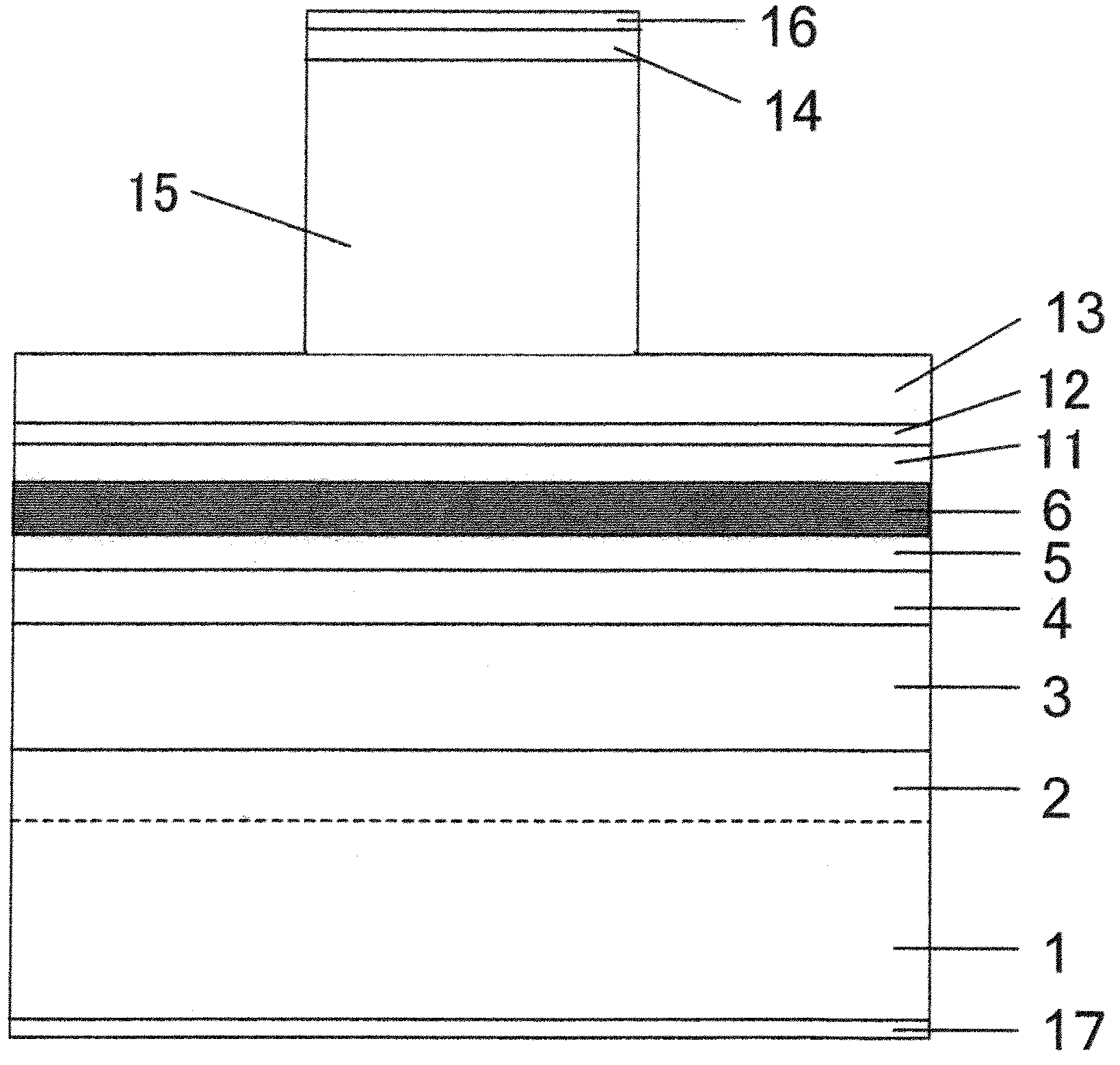
[0053]A first embodiment of the present invention will be described with reference to a cross-sectional view (FIG. 11) and a band structure drawing (FIG. 12). By the metal-organic chemical vapor deposition, a Si-doped n-type GaN buffer layer 2 (film thickness: 1000 nm, Si concentration: 1×1018 cm−3) , a Si-doped n-type AlGaN cladding layer 3 (Al composition ratio: 0.04, film thickness: 2500 nm, Si concentration: 1×1018 cm−3), a Si-doped n-type GaN guide layer 4 (film thickness: 100 nm, Si concentration: 5×1017 cm−3), an undoped InGaN guide layer 5 (In composition ratio: 0.01, film thickness: 60 nm), and an undoped InGaN multiple quantum well active layer 6 (the number of periods: 3, In composition ratio of an undoped InGaN well layer 8: 0.20, film thickness of the layer 8: 3.0 nm, In composition ratio of GaN layer 9 and an undoped InGaN barrier layer 7: 0.02, film thickness of the layers 9 and 10: 4 nm and 10 nm) are formed on a (0001) n-type GaN substrate 1. FIG. 12 shows details o...

second embodiment

[0060]FIG. 13 is a band structure drawing in the vicinity of the active layer in the case where the present invention is applied to the undoped InGaN guide layer 5, which is a second embodiment of the present invention.

[0061]First, the Si-doped n-type GaN buffer layer 2 (film thickness: 1000 nm, Si concentration: 1×1018 cm−3), the Si-doped n-type AlGaN cladding layer 3 (Al composition ratio: 0.04, film thickness: 2500 nm, Si concentration: 1×1018 cm−3), and the Si-doped n-type GaN guide layer 4 (film thickness: 100 nm, Si concentration: 5×1017 cm−3) are sequentially formed on the (0001) n-type GaN substrate 1 by the metal-organic chemical vapor deposition through the steps similar to those of the above-described first embodiment.

[0062]Next, after an undoped InGaN guide layer 18 (In composition ratio: 0.01, film thickness: 110 nm) is grown to an intermediate point in a gas atmosphere composed of nitrogen and ammonia, a GaN layer 19 (film thickness: 2.5 nm) is grown in a gas atmospher...

third embodiment

[0065]FIG. 14 is a band structure drawing in the vicinity of the active layer in the case where the present invention is applied to the part between the undoped InGaN guide layer 5 and the undoped InGaN barrier layer 7, which is a third embodiment of the present invention.

[0066]First, the Si-doped n-type GaN buffer layer 2 (film thickness 1000 nm, Si concentration: 1×1018 cm−3) to an undoped InGaN guide layer 21 (In composition ratio: 0.01, film thickness: 120 nm) are sequentially grown on the (0001) n-type GaN substrate 1 by the metal-organic chemical vapor deposition through the steps similar to those of the above-described first embodiment.

[0067]Then, after a GaN layer (film thickness 4 nm) 22 is grown in a gas atmosphere to which hydrogen is added at 5%, the undoped InGaN barrier layer 10 (In composition ratio: 0.02, film thickness: 10 nm) is grown in a gas atmosphere to which hydrogen is not added. Thereafter, a laser structure is manufactured through the steps similar to those...


PUM


Abstract

In an InGaN-based nitride semiconductor optical device having a long wavelength (440 nm or more) equal to or more than that of blue, the increase of a wavelength is realized while suppressing In (Indium) segregation and deterioration of crystallinity. In the manufacture of an InGaN-based nitride semiconductor optical device having an InGaN-based quantum well active layer including an InGaN well layer and an InGaN barrier layer, a step of growing the InGaN barrier layer includes: a first step of adding hydrogen at 1% or more to a gas atmosphere composed of nitrogen and ammonia and growing a GaN layer in the gas atmosphere; and a second step of growing the InGaN barrier layer in a gas atmosphere composed of nitrogen and ammonia.

Description

CROSS-REFERENCE TO RELATED APPLICATION[0001]The present application claims priority from Japanese Patent Application No. JP 2008-318274 filed on Dec. 15, 2008, the content of which is hereby incorporated by reference into this application.TECHNICAL FIELD OF THE INVENTION[0002]The present invention relates to a nitride semiconductor optical device and a manufacturing technique thereof, and more particularly to a technique effectively applied to an InGaN-based nitride semiconductor optical device having a long wavelength equal to or more than that of blue (440 nm or more) and a manufacture method thereof.BACKGROUND OF THE INVENTION[0003]Conventionally, with respect to the practical wavelength regions of nitride semiconductor optical devices, the wavelength region in a practical level is about 365 nm to 550 nm in a light emitting diode and is 375 nm to 488 nm in a laser diode. In both the light emitting diode and the laser diode, device characteristics are deteriorated as the wavelengt...

Claims


Application Information

Patent Timeline
IPC IPC(8): H01S5/34H01L33/00H01L29/06
CPCB82Y20/00H01L33/0075H01S5/2009H01S5/34333H01S5/3215H01S5/3407H01S5/3213
Inventor TSUCHIYA, TOMONOBUTANAKA, SHIGEHISATERANO, AKIHISANAKAHARA, KOUJI
Owner USHIO OPTO SEMICON
Why Eureka
Try Eureka