True csp power mosfet based on bottom-source ldmos

a bottom-source metal oxide semiconductor and mosfet technology, applied in the direction of transistors, semiconductor devices, electrical apparatus, etc., can solve the problems of parasitic parasitic factors such as resistance, capacitance and inductance associated with conventional packaging techniques, and further reduce the source inductance and resistance of semiconductor power devices including the source inductance, so as to reduce the resistance and inductance of the resulting device package, the effect of improving shielding

Active Publication Date: 2010-07-01
ALPHA & OMEGA SEMICON LTD
View PDF15 Cites 33 Cited by
  • Summary
  • Abstract
  • Description
  • Claims
  • Application Information

AI Technical Summary

Benefits of technology

[0051]FIG. 9 is a cross-sectional view of the semiconductor package of FIG. 1 along line B-B′ comprising the inverted trench Vertical channel MOSFET devices of FIG. 7 according to an embodiment of the present invention. As shown in FIG. 9, the source connection 110 is formed by a wide trench with source metal 904 and conductive (e.g., tungsten) plugs 902 inside the trench to contact the buried conductive plug 722. The gate pad 112 is formed on top of a gate metal 906 electrically connected to an array of gate runners 710 via conductive plugs 738. Under the correct layout, the buried conductive plug 722 may distribute the source throughout the semiconductor device, without needing to go through the substrate, to achieve lower resistance.
[0052]The structures of the semiconductor packages described above in FIGS. 2-9 provide distributed substrate connection within

Problems solved by technology

Conventional technologies to further reduce the source inductance and resistance for semiconductor power devices including the source inductance in FET, MOSFET and JFET devices are challenged by several technical difficulties and limitations.
There are difficulties in such approaches due to the fact that typical vertical semiconductor power devices are arranged to place the drain electrode on the substrate.
Advances in semiconductor processing technology, however, have made parasitics (e.g., resistances, capacitances and inductances) associated with conventional packaging techniques more of a performance-limiting factor.
In the case of conventional flip chip technology, among other shortcomings, electrical connection to the back side of the die (for vertical semiconductors) is not easily facilitated.
These limitations become quite significant in high current applications such as power switching devices.
However, connecting dies to individual clips tends to be time consuming compared with wafer level processing.
In addition, different U-sha

Method used


Image

  • True csp power mosfet based on bottom-source ldmos
  • True csp power mosfet based on bottom-source ldmos
  • True csp power mosfet based on bottom-source ldmos

Examples


Embodiment Construction

[0030]Although the following detailed description contains many specific details for the purposes of illustration, anyone of ordinary skill in the art will appreciate that many variations and alterations to the following details are within the scope of the invention. Accordingly, the examples of embodiments of the invention described below are set forth without any loss of generality to, and without imposing limitations upon, the claimed invention.

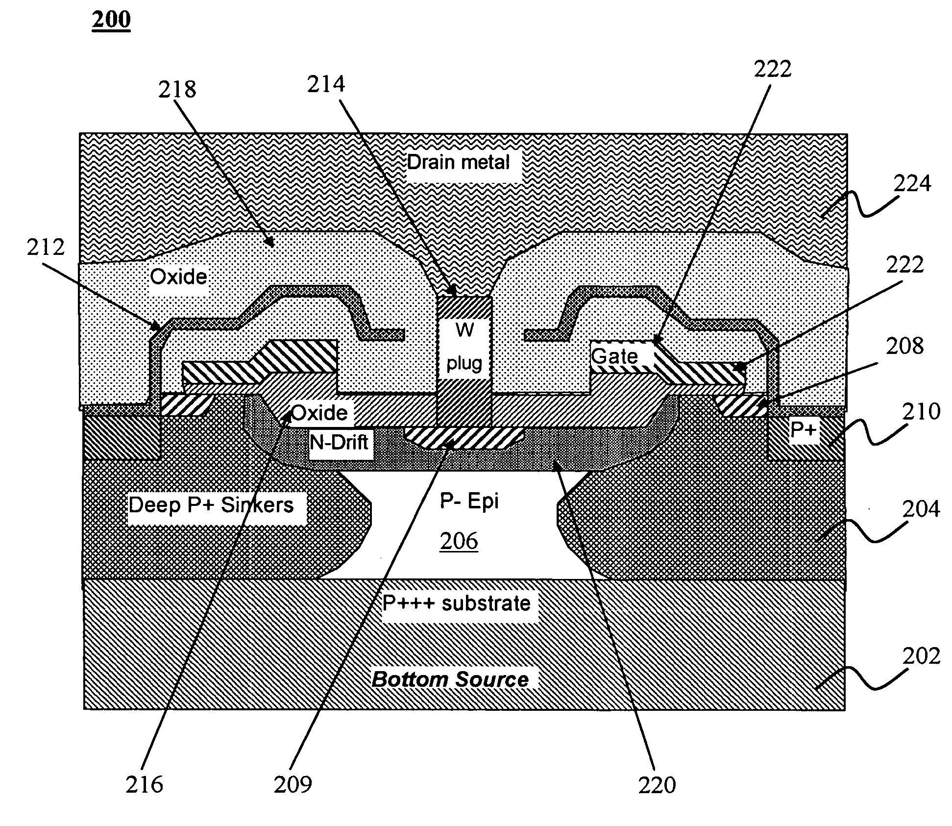
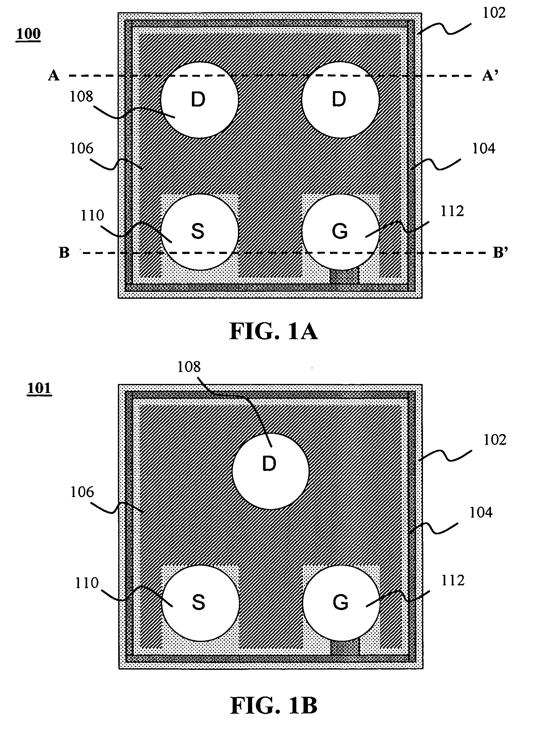
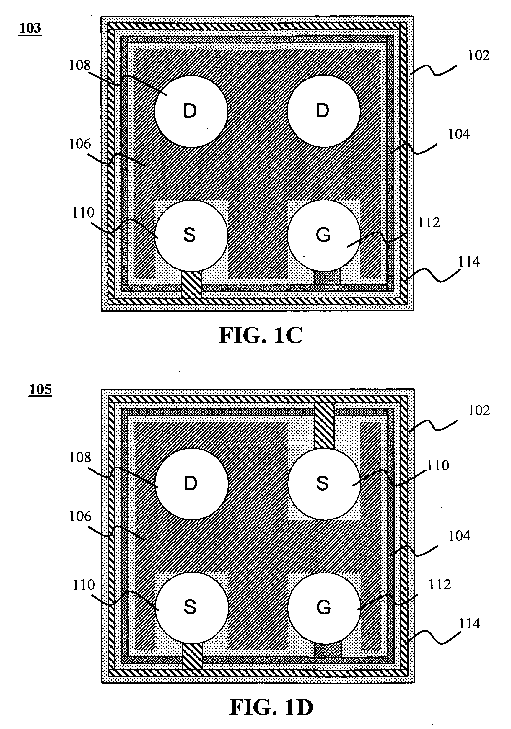
[0031]Embodiments of the present invention provide a true-CSP discrete MOSFET device using bottom-source devices with all drain, source and gate connections for the package located on a front face of the die.

[0032]According to embodiments of the present invention, a semiconductor package may comprise a semiconductor substrate, a plurality semiconductor devices formed on the semiconductor substrate, a source region disposed on a bottom of the substrate that is common to all the devices in the plurality. Each semiconductor device in the plur...


PUM


Abstract

A semiconductor package may comprise a semiconductor substrate, a MOSFET device having a plurality cells formed on the substrate, and a source region common to all cells disposed on a bottom of the substrate. Each cell comprises a drain region on a top of the semiconductor device, a gate to control a flow of electrical current between the source and drain regions, a source contact proximate the gate; and an electrical connection between the source contact and source region. At least one drain connection is electrically coupled to the drain region. Source, drain and gate pads are electrically connected to the source region, drain region and gates of the devices. The drain, source and gate pads are formed on one surface of the semiconductor package. The cells are distributed across the substrate, whereby the electrical connections between the source contact of each device and the source region are distributed across the substrate.

Description

FIELD OF THE INVENTION[0001]The invention relates generally to semiconductor power devices, and more particularly to a bottom-source metal oxide semiconductor field effect transistor (MOSFET) structure and a low cost process of chip scale package (CSP).BACKGROUND OF THE INVENTION[0002]Conventional technologies to further reduce the source inductance and resistance for semiconductor power devices including the source inductance in FET, MOSFET and JFET devices are challenged by several technical difficulties and limitations. There are ever increasing demands to reduce the source inductance and resistance in semiconductor power devices because more and more power devices are required to being used in applications that demand high efficiency, high gain, and high frequency semiconductor power devices. Reductions in source inductance can be achieved by eliminating the bond-wires in the package of a semiconductor power device. Many attempts have been made to eliminate bond-wires by configu...

Claims


Application Information

Patent Timeline
IPC IPC(8): H01L29/78H01L21/336
CPCH01L24/45H01L29/0692H01L29/402H01L29/4175H01L29/41758H01L29/41766H01L29/4236H01L29/42368H01L29/4238H01L29/456H01L29/781H01L29/7835H01L2224/04042H01L2224/05093H01L2224/05094H01L2224/45124H01L2224/45144H01L2924/01005H01L2924/01013H01L2924/01014H01L2924/01015H01L2924/01022H01L2924/01027H01L2924/01028H01L2924/01029H01L2924/01033H01L2924/01047H01L2924/0105H01L2924/01074H01L2924/01079H01L2924/01082H01L2924/014H01L2924/04941H01L2924/05042H01L2924/13091H01L2924/30105H01L2924/30107H01L2924/3011H01L2924/3025H01L2924/00014H01L24/05H01L2924/01006H01L2224/48H01L2224/05556H01L2924/13062H01L2924/00H01L2924/1306
Inventor HEBERT, FRANCOIS
Owner ALPHA & OMEGA SEMICON LTD
Why Eureka
Try Eureka