Method of producing a thin film photovoltaic system, and a thin film photovoltaic system

a technology of photovoltaic system and thin film, which is applied in the direction of photovoltaic energy generation, photovoltaics, electrical apparatus, etc., can solve the problems of only achieving plasmon resonance and not efficiently contributing to charge carrier separation, so as to achieve cost-efficient production, facilitate the effect of carrying out and reducing production costs

Inactive Publication Date: 2010-08-12
ZYLUM BETEILIGUNGSGMBH & PATENTE II
View PDF13 Cites 10 Cited by
  • Summary
  • Abstract
  • Description
  • Claims
  • Application Information

AI Technical Summary

Benefits of technology

[0008]The method is comparatively easy to carry out and enables the cost-efficient production of—even large-surface—PV modules. The selec

Problems solved by technology

Practical tests, however, showed that this plasmon resonance does not efficiently contribute to charge carrier separation since the induced oscillation propagates parallel and not perpendicular to the e

Method used


Image

  • Method of producing a thin film photovoltaic system, and a thin film photovoltaic system
  • Method of producing a thin film photovoltaic system, and a thin film photovoltaic system
  • Method of producing a thin film photovoltaic system, and a thin film photovoltaic system

Examples


Embodiment Construction

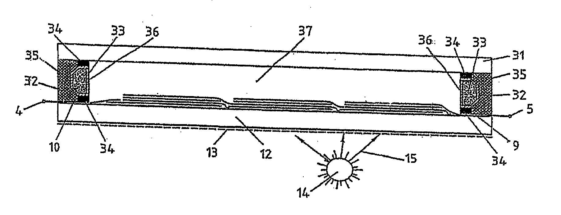
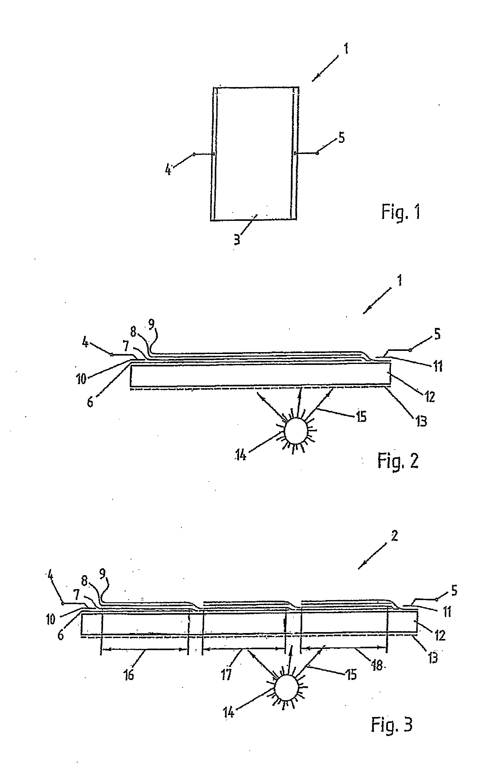
[0020]FIG. 1 shows a schematic top view of a simple thin film PV system 1 based on a monocell having the photosensitive portion 3 and the TCO (transparent conductive oxide) terminal 4 and a metallic Schottky contact 5.

[0021]If n-doped TiO2 having a thin platinum Schottky electrode is selected as the semiconductor material, a voltage of about 0.4 V can thus be achieved at the terminals 4, 5. With a typical efficiency of 3 to 12%, such a monocell is not suited for large-surface formats, since usual TCO layers (ITO (indium tin oxide), ATO (antimony tin oxide), FTO (fluorine doped tin oxide), ZnO (zinc oxide), semitransparent metallic thin films of gold, thin films based on single-wall carbon nanotubes or silver-wire thin films) have comparatively high sheet resistances and only reach values of below 10 Ω / m2 at a concurrently lower transparency to natural light.

[0022]The TEC Glass #8 / 3 from the Pilkington Specialty Glass Products Company, Toledo, Ohio 43697-0799, USA, for instance, has ...


PUM

PropertyMeasurementUnit
Thicknessaaaaaaaaaa
Thicknessaaaaaaaaaa
Thicknessaaaaaaaaaa

Abstract

A method of producing a thin film photovoltaic system (2) having a two-dimensional metal chalcogenide compound semiconductor layer (7) as an absorber of sunlight and a metal layer (8) applied to the metal chalcogenide compound semiconductor layer is provided, wherein the metal chalcogenide compound semiconductor layer (7) and the metal layer (8) form a Schottky contact at their contact face. The method is characterized in that the metal chalcogenide compound semiconductor layer (7) is produced by applying a dispersion containing nanoscale particles having a diameter of about 3 nm to about 30 nm to a transparent substrate material (12), wherein the layer thickness of the metal chalcogenide compound semiconductor layer (7) applied to the substrate material ranges from about 150 nm to about 2500 nm.

Description

BACKGROUND OF THE INVENTION[0001]The invention relates to a method of producing a thin film photovoltaic system, to a thin film photovoltaic system and its use, particularly in a photovoltaic module for converting solar energy into electrical energy.[0002]A reaction cell for photo-electrochemically producing hydrogen gas is known from German Patent DE 10 2004 012 303 B3. In the described technical solution, a housing filled with an aqueous electrolyte is provided in which a first electrode consisting of a doped semiconductor material, e.g. TiO2 or SrTiO3, and a second electrode consisting of a noble or semi-precious metal, or oppositely doped as compared to the first electrode, are provided. The two electrodes are connected to one another in an electrically conducting manner and are irradiated by a light source during operation. The electrodes are arranged such that the reaction cell is divided into two chambers which are interconnected in an ion-conducting manner. The hydrogen form...

Claims


Application Information

Patent Timeline
IPC IPC(8): H01L27/142H01L31/18H01L31/07
CPCB32B17/10018B32B17/10761B32B17/10788B32B2327/12H01L21/02551H01L21/02568Y02E10/541H01L21/02628H01L31/0296H01L31/032H01L31/0392H01L31/07H01L31/1836H01L21/02601H01L31/03925Y02E10/50
Inventor OSTERMANN, DIETER
Owner ZYLUM BETEILIGUNGSGMBH & PATENTE II
Why Eureka
Try Eureka