
Field effect transistor

Inactive Publication Date: 2010-09-09
CANON KK
View PDF22 Cites 21 Cited by
  • Summary
  • Abstract
  • Description
  • Claims
  • Application Information

AI Technical Summary

Benefits of technology

[0016]The present invention has been made in view of the above-mentioned problem, it is therefore an object of the present invention to provide a thin film transistor that uses an amorphous oxide containing a few elements, that has an excellent environmental stability such as one inflicted during storage in atmospheric air, and that has a low sensitivity with respect to visible light.
[0018]According to the present invention, the field effect transistor having excellent characteristics can be realized by forming the channel layer from the amorphous oxide that contains In and Mg (or Al). Especially a transistor with low visible light sensitivity, in other words, very stable against light irradiation, can be obtained. Thus, when applied to a display, the TFT can operate stably in a bright place as well.
[0019]Further, the transistor of the present invention undergoes substantially no changes in characteristics with time during storage in atmospheric air, and therefore has an excellent environmental stability.

Problems solved by technology

However, it is difficult to produce an amorphous silicon TFT, a polysilicon TFT, and other TFT's on a substrate such as a plastic plate or foil since high-temperature processing is demanded for device production.
However, pentacene and other organic semiconductors have problems of being low in thermal stability (<150° C.) and being toxic (carcinogenic), and therefore have not succeeded in producing a device fit for practical use.
However, ZnO cannot form a stable amorphous phase at room temperature and forms a polycrystalline phase instead, which causes electron scattering in the polycrystalline grain boundaries and makes it difficult to increase the electron mobility.
Therefore, TFT characteristics may scatter from device to device and lot to lot.
When the channel layer of a TFT has a certain level of optical sensitivity, the electric characteristics of the channel layer are varied depending on the amount of light irradiation, with the result that the operation of the TFT is made unstable.
One way to avoid this adverse effect of light is providing the display with a light-shielding layer, but completely eliminating stray light puts severe limitation on the structure of the display.

Method used


Image

  • Field effect transistor
  • Field effect transistor
  • Field effect transistor

Examples


example 1

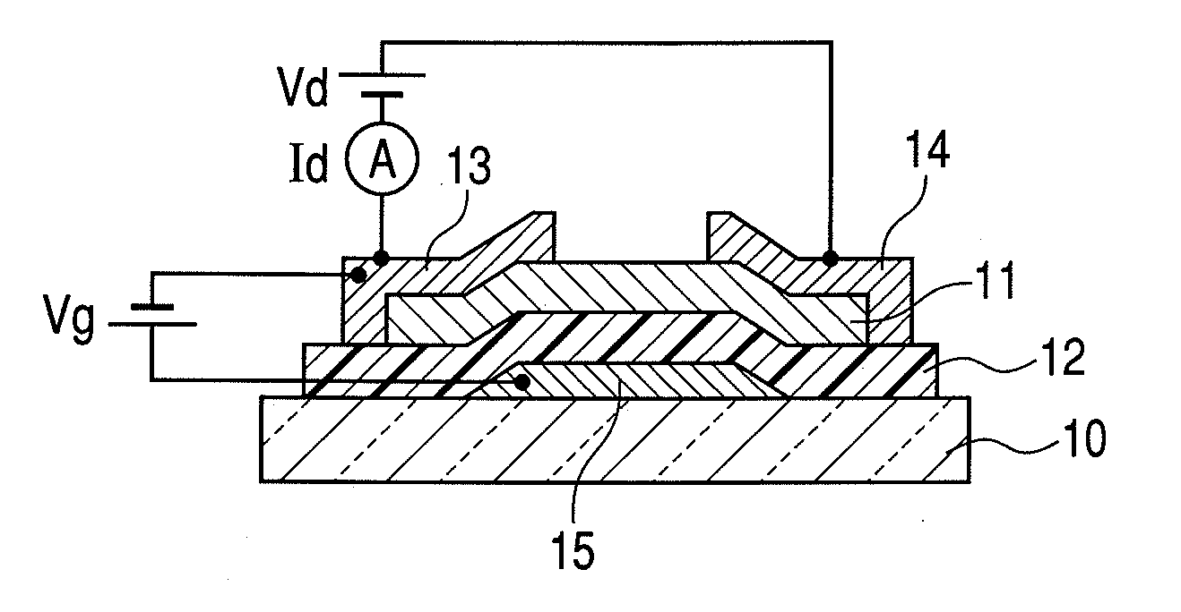
[0084]In this example, the top-gate TFT device illustrated in FIG. 8A was manufactured with an In—Mg—O-based amorphous oxide as a channel layer.

[0085]First, an In—Mg—O-based amorphous oxide film was formed as the channel layer on a glass substrate (1737 manufactured by Corning Incorporated). The film was formed by high-frequency sputtering in a mixed atmosphere of argon gas and oxygen gas with the use of an apparatus illustrated in FIG. 10. In FIG. 10, a sample, a target, a vacuum pump, a vacuum gauge, and a substrate holder are denoted by reference numerals 51, 52, 53, 54, and 55, respectively. A gas flow rate controller 56 is provided for each gas introduction system. A pressure controller and a film formation chamber are denoted by reference numerals 57 and 58, respectively. The vacuum pump 53 is an exhaust unit for exhausting the interior of the film formation chamber 58. The substrate holder 55 is a unit for keeping the substrate on which the oxide film is to be formed within t...

example 2

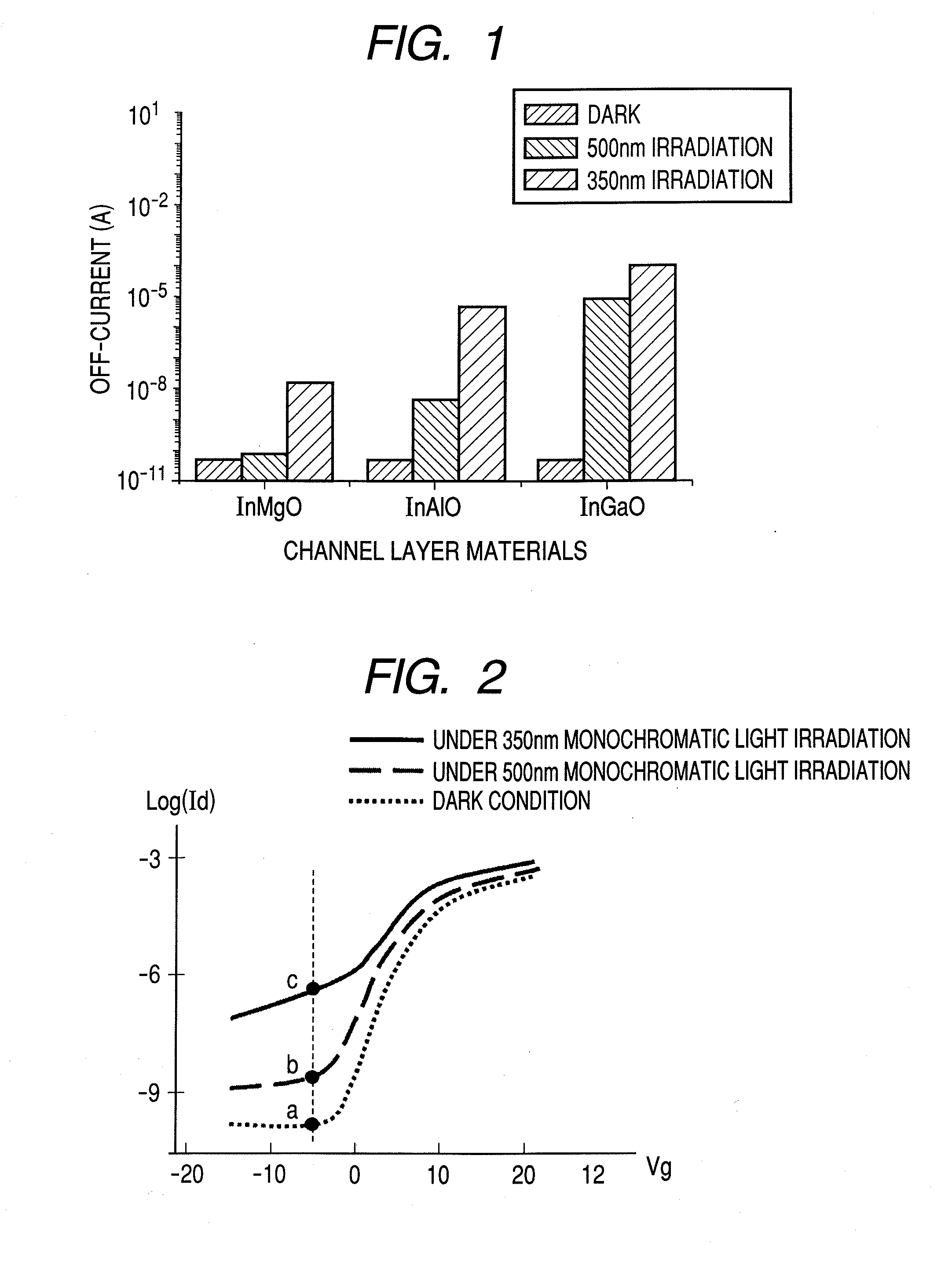
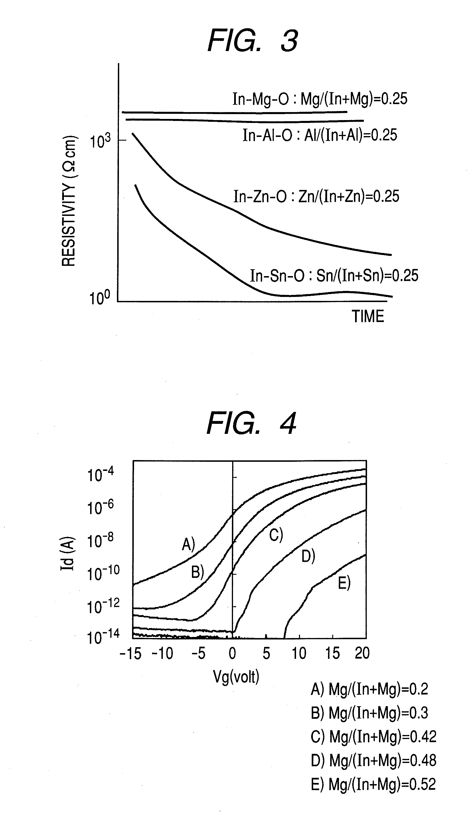
[0104]In this example, the In—Mg composition dependency was examined in a thin film transistor with a channel layer that contains In and Mg as major components.

[0105]This example employed the combinatorial method for TFT fabrication (channel layer formation) in order to examine the material composition dependency of the channel layer. In other words, TFT compositional library was made with the use of a method of forming, by sputtering, thin films of oxides varied in composition on a single substrate. However, it does not need to be this combinatorial method, and targets of a given composition may be prepared to form a film, or thin films of desired compositions may be formed by controlling the input power for multiple targets separately.

[0106]An In—Mg—O film was formed with the use of a ternary grazing incidence sputtering apparatus. With the target positioned at an angle with respect to the substrate, the composition of a film on the substrate surface is varied due to a difference ...

example 3

[0122]In this example, a channel layer was formed from an In—Al—O-based amorphous oxide, and the top-gate TFT device illustrated in FIG. 8A that used this channel layer was manufactured and evaluated by the same method that was employed in Example 1.

[0123]2-inch sized targets of In2O3 and Al2O3 (purity: 99.9%) were used to form an In—Al—O film by simultaneous sputtering. The input RF power was 60 W and 180 W for the former and latter targets. The atmosphere in the film formation was set such that the total pressure was 0.4 Pa and the gas flow rate ratio was Ar:O2=150:1. The film formation rate and the substrate temperature were set to 11 nm / min. and 25° C., respectively. Subsequently, the film was subjected to an annealing process for 30 minutes at 280° C. in atmospheric air.

[0124]A glance angle X-ray diffraction (thin film method, incident angle: 0.5°) was performed on the surface of the obtained film. No obvious diffraction peaks were detected, which indicated that the formed In—A...


PUM

PropertyMeasurementUnit
Ratioaaaaaaaaaa

Abstract

A field effect transistor includes at least a channel layer, a gate insulation layer, a source electrode, a drain electrode, and a gate electrode. The channel layer is formed from an amorphous oxide material that contains at least In and Mg, and an element ratio, expressed by Mg / (In+Mg), of the amorphous oxide material is 0.1 or higher and 0.48 or lower.

Description

TECHNICAL FIELD[0001]The present invention relates to a field effect transistor using an amorphous oxide. More particularly, the present invention relates to a field effect transistor using an amorphous oxide as a channel layer.BACKGROUND ART[0002]Field effect transistors (FETs) are electronic active devices with a gate electrode, a source electrode, and a drain electrode that control electric current between the source electrode and the drain electrode by controlling the flow of electric current into a channel layer through voltage application to the gate electrode. FETs that use as the channel layer a thin film formed on an insulated substrate such as a ceramic, glass, or plastic substrate, in particular, are called thin film transistors (TFTs).[0003]The above-mentioned TFTs are formed by using a thin film technology, and hence the TFTs have an advantage of being easily formed on the substrate having a relatively large area, and therefore are widely used as a driving device for a ...

Claims


Application Information

Patent Timeline
IPC IPC(8): H01L33/16H01L29/786
CPCH01L29/7869C23C14/086
Inventor IWASAKI, TATSUYAITAGAKI, NAHO
Owner CANON KK
Features
  • Generate Ideas
  • Intellectual Property
  • Life Sciences
  • Materials
  • Tech Scout
  • Unparalleled Data Quality
  • Higher Quality Content
  • 60% Fewer Hallucinations
Learn More