

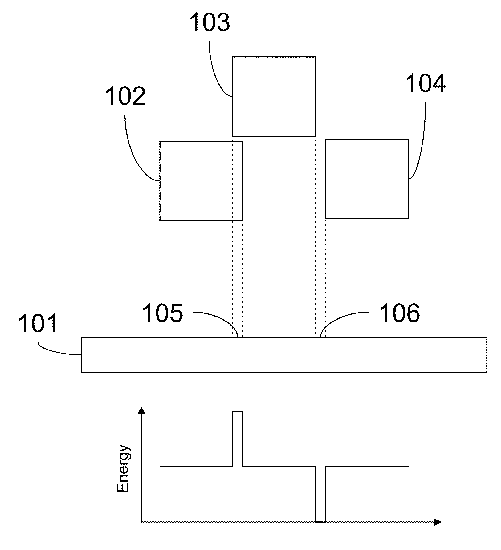
Mirror arrays for maskless photolithography and image display
a technology of mirror arrays and photolithography, applied in the direction of photomechanical equipment, instruments, originals for photomechanical treatment, etc., can solve the problems of difficult use of contact printing methods, discouraging industry adoption, mask contamination, etc., and achieve the effect of low cost and lower cos
- Summary
- Abstract
- Description
- Claims
- Application Information
AI Technical Summary
Benefits of technology
Problems solved by technology
Method used
Image

Examples
example 1
Digital Micromirror Devices and Use of Dielectric Reflectors
[0076]Micromirror arrays were researched during the 1980s for the optical purposes such as light processing, image display, and optical switches. One of the applications of micromirror arrays is the DMD (digital micromirror device, Texas Instruments) for DLP (Digital Light Processing) projection systems. A DMD is made of approximately one million micromirrors, which reflect light in the intended directions under the control of a processor. By controlling the reflection of each mirror, a projection image is generated after some optical systems. FIG. 14 shows a schematic illustration of a DMD device and its SEM image (M. Douglass, Reliability testing and characterization of MEMS / MOEMS II, Proceedings of SPIE vol. 4980, 2003). The micromirror arrays in the DMD chip are fabricated by a microfabrication process.
[0077]DMD arrays are useful as light modulators for projection display products. There, white light is illuminated on t...
example 2
Micromirror Arrays for High Fluence Conditions Using Dielectrics
[0080]Conventional micromirrors are fabricated on a silicon substrate, and a metal such as aluminum, or gold is used as a mirror layer. The metal itself can be the structural material of the whole micromirror or can be coated on top of another structural material. However, if the illumination intensity increases beyond a particular threshold, the metal layer and / or the entire mirror structure can be damaged by absorbed heat. Therefore, the illumination intensity limits the application of the micromirror arrays.
[0081]Use of a high reflectivity dielectric coating on top of the mirror structure or on top of the metal mirror limits the amount of heat absorbed by the mirror. Accordingly, the illumination intensity on the micromirror can be increased further. With higher useful illumination intensities on micromirror structures, the application of micromirrors can be broadened.
[0082]In the use of micromirrors for display prod...
example 3
Polymer Micromirror Arrays for High Fluence Conditions Using Dielectrics
[0083]In the fabrication of conventional micromirror structures, reflective metal layers are deposited on top of the mirror structures to gain higher reflectivity. Silicon, aluminum or other kinds of solid materials are used for the structure of micromirror arrays. However, the most common way to deposit such materials is sputtering or chemical vapor deposition (CVD), which requires expensive vacuum equipment, long process times, frequent maintenance and expensive precursors. In order to pattern the metal layer, a wet etch system with metal etchant is generally required.
[0084]Polymer materials can be used as structural members of micromirrors, reducing the production costs because the process can be simplified. For the coating of the polymer material, spin coating and baking processes can be readily used which are much faster and cheaper. The equipment used in such processes is also much cheaper than the common ...
PUM
| Property | Measurement | Unit |
|---|---|---|
| Temperature | aaaaa | aaaaa |
| Fraction | aaaaa | aaaaa |
| Fraction | aaaaa | aaaaa |
Abstract
Description
Claims
Application Information