Metal wiring structures for uniform current density in c4 balls

a technology of current density and metal wiring, which is applied in the field of metal wiring structures for bonding pads, can solve problems such as non-uniformity of vias, and achieve the effect of facilitating uniform current density distribution and improving reliability of c4 balls

Active Publication Date: 2010-10-21
GLOBALFOUNDRIES US INC
View PDF10 Cites 37 Cited by
  • Summary
  • Abstract
  • Description
  • Claims
  • Application Information

AI Technical Summary

Benefits of technology

[0007]The present invention enhances reliability of a C4 ball by providing a metal wiring structure that facilitates uniform current density distribution within the C4 ball.
[0008]In the present invention, a sub-pad assembly of metal structures are provided, which is located directly underneath a metal pad. The sub-pad assembly includes an upper level metal line structure abutting the metal pad, a lower level metal line structure located underneath the upper level metal line structure, and a set of metal vias that provide electrical connection between the lower level metal line structure located underneath the upper level metal line structure. The set of metal vias are distributed to provide a higher current density at the center portion of the metal pad than at the peripheral portion of the metal pad that contacts a C4 ball. After a C4 ball is bonded to the metal pad, the geometry of the sub-pad assembly causes more current through the center of the metal pad so that the current density in the C4 ball becomes uniform, thereby reducing electromigration therein.
[0012]Further, the present invention enhances reliability of a C4 ball by providing a metal pad structure having a set of integrated metal vias that are segmented and distributed to facilitate uniform current density distribution within the C4 ball. The area1 density of the cross-sectional area in the plurality of metal vias is higher at the center portion of the metal pad than at the peripheral portion of the planar portion of the metal pad than at a peripheral region of the planar portion of the metal pad. After a C4 ball is bonded to the metal pad, the distribution of the variation in the area1 density of the cross-sectional area causes more current through the center of the metal pad so that the current density in a C4 ball thereupon becomes uniform, thereby reducing electromigration within the C4 ball.

Problems solved by technology

Further, the set of metal vias may have a non-uniform spacing between neighboring metal vias in two different directions in a horizontal plane, in which spacing between neighboring metal vias are modulated in both directions.

Method used


Image

  • Metal wiring structures for uniform current density in c4 balls
  • Metal wiring structures for uniform current density in c4 balls
  • Metal wiring structures for uniform current density in c4 balls

Examples


first embodiment

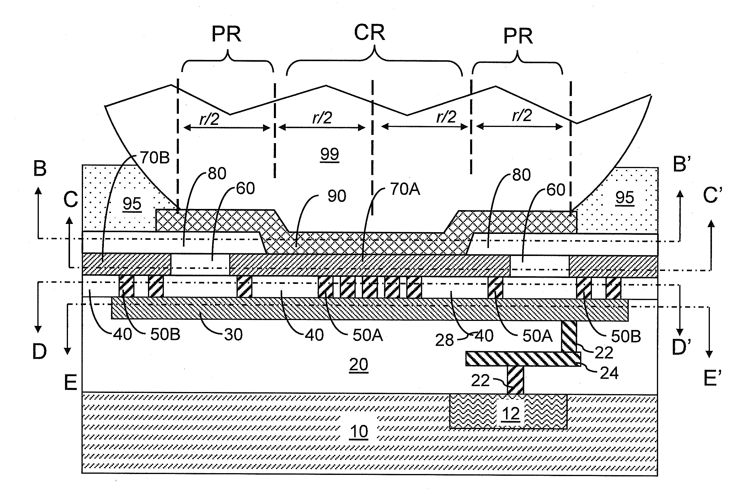
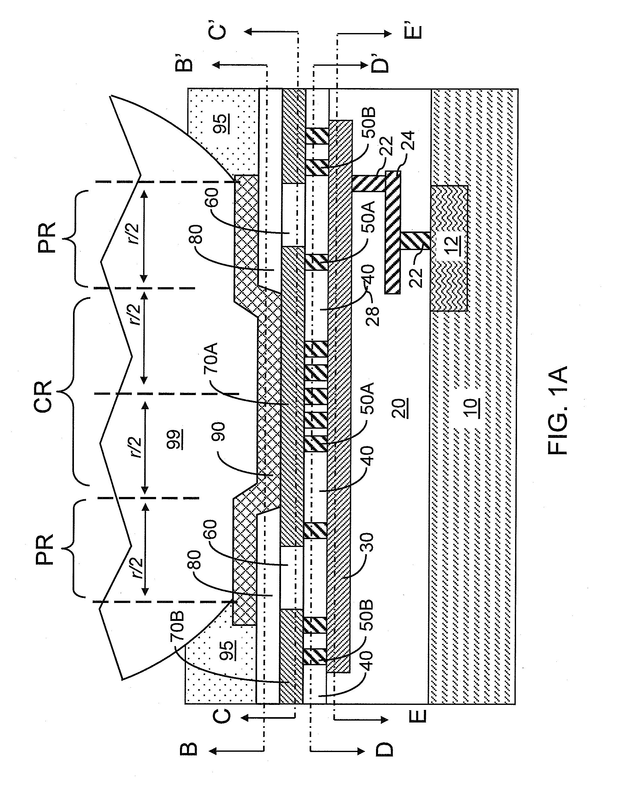
[0039]Referring to FIGS. 1A-1E, a first exemplary structure according to the present invention is shown. The first exemplary structure includes a substrate 10 and at least one semiconductor device 12 formed therein. The substrate 10 may be a semiconductor substrate comprising a semiconductor material such as silicon, a silicon germanium alloy region, silicon, germanium, a silicon-germanium alloy region, a silicon carbon alloy region, a silicon-germanium-carbon alloy region, gallium arsenide, indium arsenide, indium gallium arsenide, indium phosphide, lead sulfide, other III-V compound semiconductor materials, and II-VI compound semiconductor materials. The substrate may be a single crystalline semiconductor substrate.

[0040]The at least one semiconductor device 12 may include at least one of a field effect transistor, a bipolar transistor, a diode, a resistor, a capacitor, and an inductor. At least one dielectric layer 20 is located on the at least one semiconductor device 12. The at...

eighth embodiment

[0074]Referring to FIGS. 15A-15D, an eighth exemplary structure according to the present invention is shown. The eighth exemplary structure includes a substrate 610 and at least one semiconductor device 612 formed therein. The substrate 610 may be a semiconductor substrate comprising a semiconductor material such as silicon, a silicon germanium alloy region, silicon, germanium, a silicon-germanium alloy region, a silicon carbon alloy region, a silicon-germanium-carbon alloy region, gallium arsenide, indium arsenide, indium gallium arsenide, indium phosphide, lead sulfide, other III-V compound semiconductor materials, and II-VI compound semiconductor materials. The substrate may be a single crystalline semiconductor substrate.

[0075]The at least one semiconductor device 612 may include at least one of a field effect transistor, a bipolar transistor, a diode, a resistor, a capacitor, and an inductor. At least one dielectric layer 620 is located on the at least one semiconductor device ...

tenth embodiment

[0091]The plurality of metal vias 690X of the tenth embodiment is arranged in a two-dimensional array including a plurality of one-dimensional arrays in radial directions that intersect one another at a center point underneath the center region CR. The spacing between neighboring metal vias of the plurality of metal vias 690X is less under the center region CR than under the peripheral regions PR in each of the plurality of one-dimensional arrays. The sum of the center region CR and the peripheral regions PR is the same as the total contact area between the metal pad 690 and the C4 ball 699 (See FIGS. 15A and 16A).

[0092]Referring to FIG. 18, a eleventh exemplary structure according to a eleventh embodiment of the present invention is shown. The eleventh exemplary structure is derived from the eighth or ninth exemplary structure by substituting a plurality of metal vias 690Y of a different type for the plurality metal vias 690V of the eighth embodiment or for the plurality of metal v...


PUM

PropertyMeasurementUnit
lengthaaaaaaaaaa
thicknessesaaaaaaaaaa

Abstract

In one embodiment, a sub-pad assembly of metal structures is located directly underneath a metal pad. The sub-pad assembly includes an upper level metal line structure abutting the metal pad, a lower level metal line structure located underneath the upper level metal line structure, and a set of metal vias that provide electrical connection between the lower level metal line structure located underneath the upper level metal line structure. In another embodiment, the reliability of a C4 ball is enhanced by employing a metal pad structure having a set of integrated metal vias that are segmented and distributed to facilitate uniform current density distribution within the C4 ball. The area1 density of the cross-sectional area in the plurality of metal vias is higher at the center portion of the metal pad than at the peripheral portion of the planar portion of the metal pad.

Description

FIELD OF THE INVENTION[0001]The present invention relates to semiconductor structures, and particularly, to metal wiring structures for bonding pads and methods of manufacturing the same.BACKGROUND OF THE INVENTION[0002]Once formation of semiconductor devices and interconnects on a semiconductor wafer (substrate) is completed, the semiconductor wafer is diced into semiconductor chips, or “dies.” Functional semiconductor chips are then packaged to facilitate mounting on a circuit board. A package is a supporting element for the semiconductor chip that provides mechanical protection and electrical connection to an upper level assembly system such as the circuit board. One typical packaging technology is Controlled Collapse Chip Connection (C4) packaging, which employs C4 balls each of which contacts a C4 pad on the semiconductor chip and another C4 pad on a packaging substrate. The packaging substrate may then be assembled on the circuit board.[0003]Each C4 pad is a contiguous metal p...

Claims


Application Information

Patent Timeline
Patent Type & Authority Applications(United States)
IPC IPC(8): H05K1/00
CPCH01L23/5226H01L24/03H01L24/05H01L24/13H01L2224/036H01L2224/0391H01L2224/05006H01L2224/05022H01L2224/05094H01L2224/05095H01L2224/05098H01L2224/05124H01L2224/05147H01L2224/05558H01L2224/05559H01L2224/05567H01L2224/05572H01L2224/05624H01L2224/11334H01L2224/13022H01L2224/13099H01L2924/01013H01L2924/01015H01L2924/01029H01L2924/01032H01L2924/01033H01L2924/01049H01L2924/01059H01L2924/01074H01L2924/01078H01L2924/01082H01L2924/10329H01L2924/19041H01L2924/19042H01L2924/19043H01L2924/01005H01L2924/01006H01L2924/01019H01L2924/01023H01L2924/01024H01L2924/01047H01L2224/13007H01L2224/0401H01L2924/1306H01L2924/1305H01L2924/00014H01L2924/0002H01L2924/00H01L2224/05552
Inventor DAUBENSPECK, TIMOTHY H.SAUTER, WOLFGANGSULLIVAN, TIMOTHY D.WRIGHT, STEVEN L.SPROGIS, EDMUND
Owner GLOBALFOUNDRIES US INC
Why Eureka
Try Eureka