

Electrically conductive bonding material, method of bonding with the same, and semiconductor device bonded with the same
a technology of electrically conductive bonding and bonding method, which is applied in the direction of semiconductor/solid-state device details, non-metal conductors, conductors, etc., can solve the problems of inferior to those achieved by metal bonded interfaces, heat dissipation capacity and bonding reliability, and conductive adhesives, etc., to achieve high heat dissipation and heat resistance. high
- Summary
- Abstract
- Description
- Claims
- Application Information
AI Technical Summary
Benefits of technology
Problems solved by technology
Method used
Image

Examples
example 1
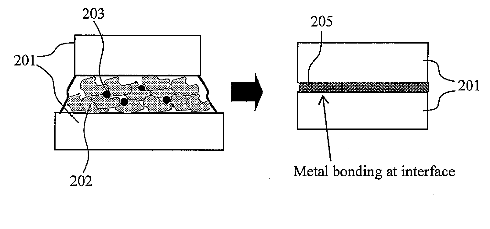
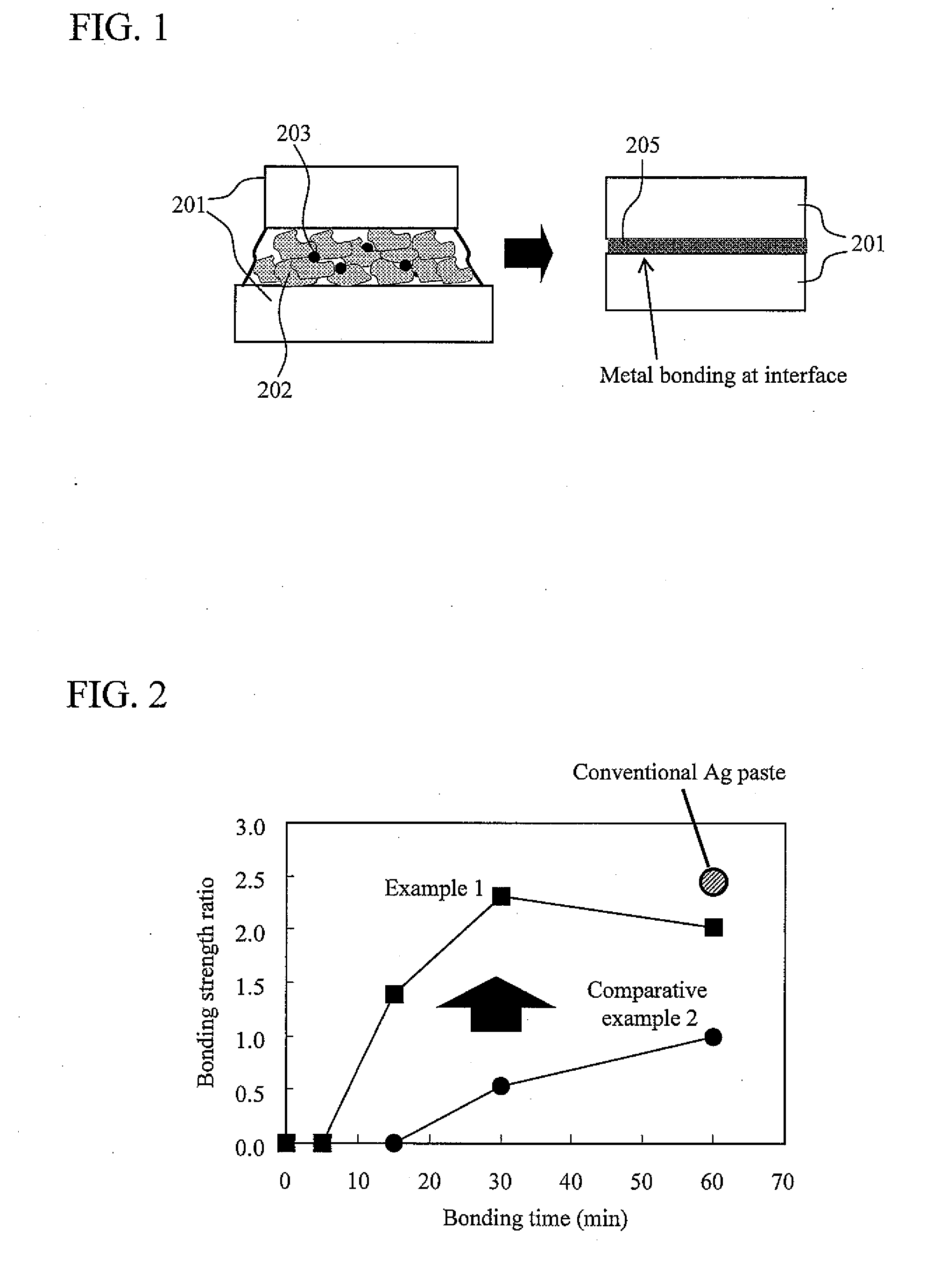
[0090]In Example 1, 0.9 g of silver flakes having an average particle size of about 1 μM, an average thickness of about 0.5 μM, and an aspect ratio of about 2.0, coated with 1.0 wt % stearic acid, 0.1 g of silver oxide (Ag2O) particles having an average particle size of about 2 μm, and 0.2 g of ethanol (made by Wako Pure Chemical Industries) as an organic solvent were used. These were blended with a mortar for about one hour to make an electrically conductive bonding material.
[0091]As Comparative Example 1, a conventional silver paste which is available in the market was used. As Comparative Example 2, an electrically conductive bonding material was made by blending 100 mass parts of silver flakes having an average particle size of about 1 μm, an average thickness of about 0.3 μm, and an aspect ratio of about 2.0, coated with 1.0 wt % stearic acid, into 20 mass parts of ethanol with a mortar for about 10 minutes.
[0092]Subsequently, after bonding was performed with the electrically c...
example 2
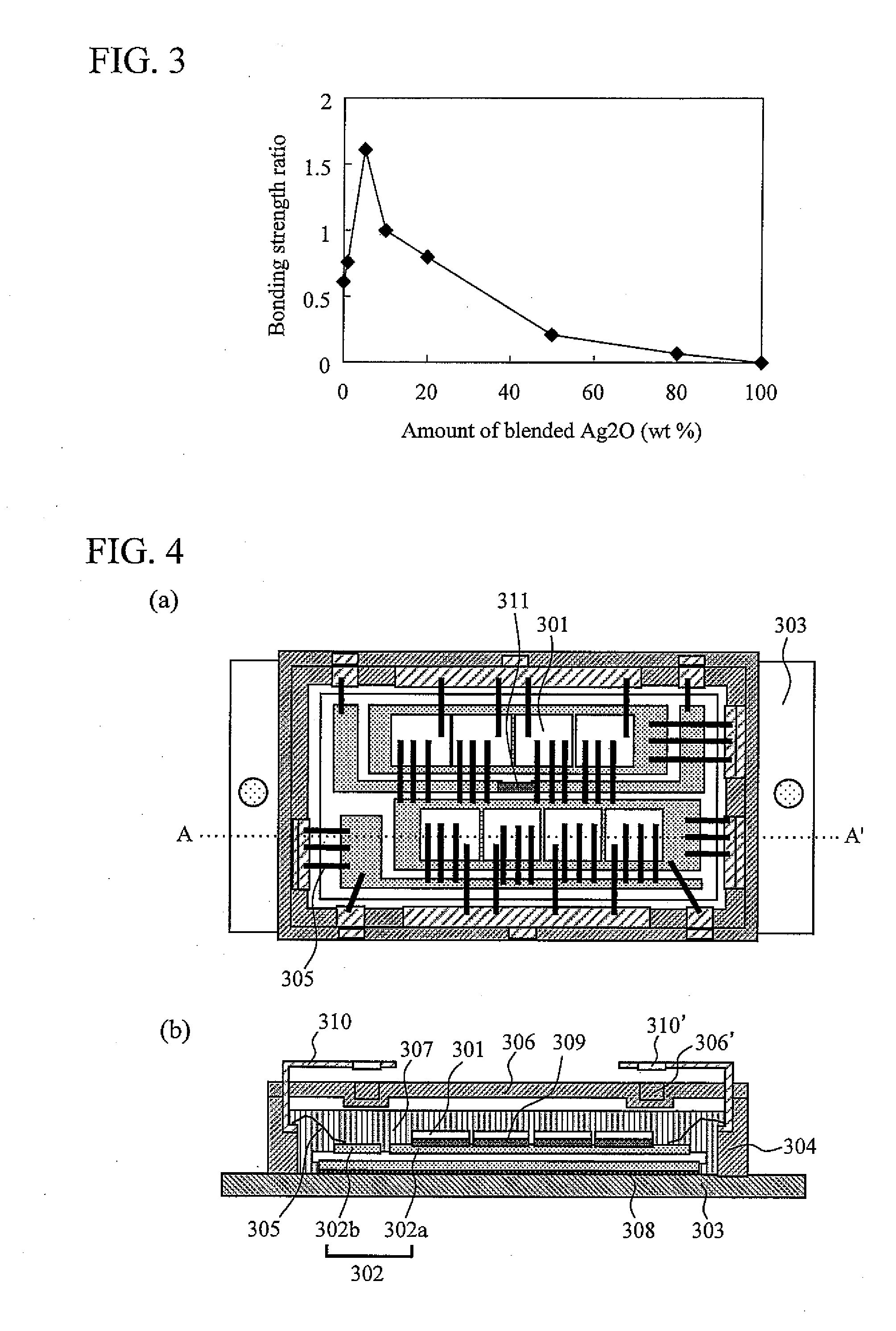
[0096]In Example 2, silver flakes having an average particle size of about 1 μm, an average thickness of about 0.5 μm, and an aspect ratio of about 2.0 were used. The specimens composed of silver flakes coated with 1.0 wt % stearic acid and silver oxide (Ag2O) particles having an average particle size of about 2 μm in a different blended ratio by weight of 95 to 5, 90 to 10, 80 to 20, or 50 to 50 were made. Furthermore, 100 mass parts of the specimens were blended into 20 mass parts of ethanol (made by Wako Pure Chemical Industries) as an organic solvent with a mortar for about 1 hour to make 1 g of the electrically conductive bonding materials, respectively. Subsequently, strength in shear was measured. The topside and downside test specimens for the measurement have a diameter of 5 mm and a thickness of 2 mm, and a diameter of 10 mm and a thickness of 5 mm, respectively. The surface of the specimens was plated with Ag. After the electrically conductive bonding materials of Example...
application example 1
[0101]FIG. 4 shows a structure of a non-insulated semiconductor device of an Application Example of the present invention. FIG. 4 (A) is a top view and FIG. 4 (B) is a cross-sectional view, taken along the line A-A′ in FIG. 4 (A). After a semiconductor element (MOSFET) 301 and a ceramic insulating substrate 302 are mounted on the ceramic insulating substrate 302 and a base member 303, respectively, an epoxy resin case 304, a bonding wire 305, and an epoxy resin lid 306 were disposed where the case was filled with silicone gel resin 307. The ceramic insulating substrate 302 on the base member 303 is bonded with a bonding layer 308 composed of the electrically conductive bonding material of Example 1, and the eight MOSFET elements 301 of Si on a copper plate 302a of the ceramic insulating substrate 302 is bonded with a bonding layer 309 composed of the electrically conductive bonding material of Example 1. For bonding with the bonding layers 308 and 309, the electrically conductive bo...
PUM
| Property | Measurement | Unit |
|---|---|---|
| particle size | aaaaa | aaaaa |
| particle size | aaaaa | aaaaa |
| boiling point | aaaaa | aaaaa |
Abstract
Description
Claims
Application Information