

Bottom source NMOS triggered zener clamp for configuring an ultra-low voltage transient voltage suppressor (TVS)
a transient voltage suppressor and bottom source technology, applied in the direction of emergency protective circuit arrangements, transistors, etc., can solve the problems of large area to reduce resistance, uncontrollable high voltage may accidentally strike the circuit, and the diodes are very resistive, so as to improve the structure of the tv device, improve clamping, and reduce the effect of voltag
- Summary
- Abstract
- Description
- Claims
- Application Information
AI Technical Summary
Benefits of technology
Problems solved by technology
Method used
Image

Examples
Embodiment Construction
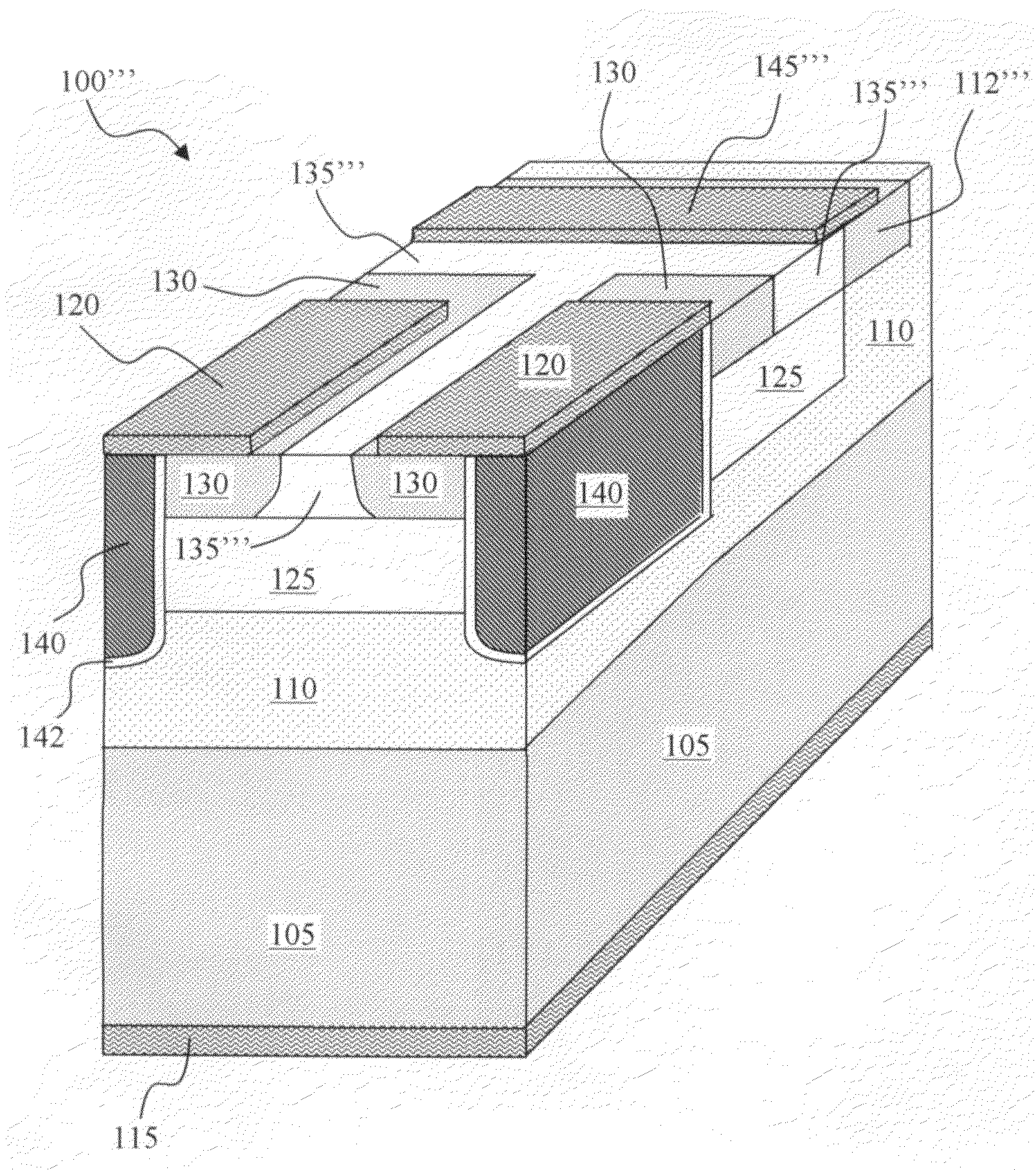
[0031]FIGS. 4A and 4B show a cross sectional view and the corresponding equivalent circuit elements respectively of a TVS device 100 of this invention. FIG. 4C is an I-V diagram that shows the current conduction and voltage characteristics of the TVS device 100. The TVS device 100 is formed in a N+ substrate 105 supporting a N-epitaxial layer 110 thereon with a anode terminal 115 disposed on the bottom and an cathode terminal 120 disposed on the top surface of the substrate that is contacted to a N+ drain / collector region 130. In addition to a TVS diode 150, the device also contains a NMOSFET 160 and a NPN bipolar transistor 170, as shown in the equivalent circuit 100. The connectivity of the terminals of the NMOS 160 and NPN bipolar transistor 170 in this structure are explained next. The TVS device structure 100 includes a surface P+ body contact region 135 on top of a P-body region 125. The surface P+ body contact region 135 is connected to the anode / source / emitter terminal using...
PUM
 Abstract
Description
Claims
Application Information