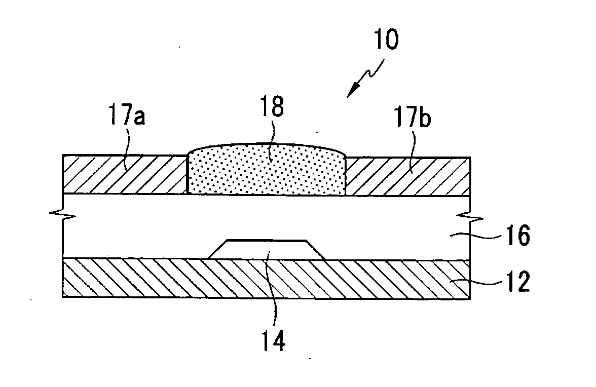
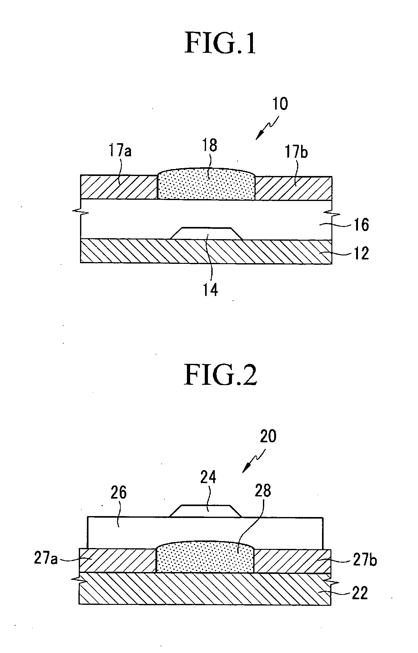
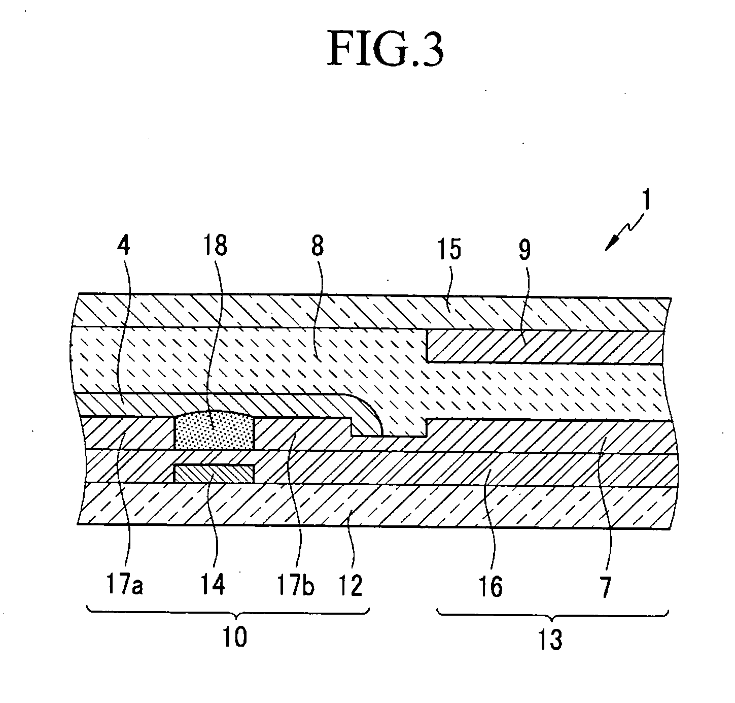
Organic semiconductor polymer, transistor including an organic semiconductor polymer and methods of fabricating the same

a technology of organic semiconductors and semiconductor polymers, which is applied in the direction of semiconductor devices, solid-state devices, thermoelectric devices, etc., can solve the problems of difficult application of conventional amorphous silicon thin films to polymer substrates for flexible displays, and achieve the effects of increasing charge mobility, electrical stability and/or air stability, and increasing charge mobility

Active Publication Date: 2011-01-06
SAMSUNG ELECTRONICS CO LTD
View PDF13 Cites 13 Cited by
  • Summary
  • Abstract
  • Description
  • Claims
  • Application Information

AI Technical Summary

Benefits of technology

[0013]Example embodiments provide an organic semiconductor polymer, which imparts increased charge mobility, electrical stability and / or air stability, and a method of fabricating the same using a solution-based process.
[0014]Example embodiments provide a transistor including an organic semiconductor polymer, which has increased charge mobility, electrical stability and / or air stability, and a method of fabricating the same using a solution-based process.

Problems solved by technology

If depositing the conventional amorphous silicon thin film transistor on a substrate, there are limits in carrying out the process at a high temperature of about 300° C., making it difficult to apply the conventional amorphous silicon thin film to a polymer substrate for a flexible display.

Method used


Image

  • Organic semiconductor polymer, transistor including an organic semiconductor polymer and methods of fabricating the same
  • Organic semiconductor polymer, transistor including an organic semiconductor polymer and methods of fabricating the same
  • Organic semiconductor polymer, transistor including an organic semiconductor polymer and methods of fabricating the same

Examples


example 1

Example 1-1

Monomer Synthesis

[0141]

[0142]As shown in Reaction Scheme (2), 2-bromo-3-dodecylthiophene (compound (1), 19.0-g, 57.5-mmol) is reacted with an excessive amount (10.3-g, 115.0-mmol) of copper cyanide (CuCN) to provide 2-cyano-3-dodecylthiophene (compound (2), yield: 71%). The obtained 2-cyano-3-dodecylthiophene and a small amount (about 0.1 equivalents) of diethylamine are dissolved in dimethylformamide (DMF), and then bubbled with H2S gas at −70° C. for about 40 minutes. The mixture is heated and reacted at about 60° C. for 2 hours. Then, the mixture is extracted with ethylacetate and water 2 or 3 times, and washed and dried to provide 2-thiocarbamyl-3-dodecylthiophene (compound (3), yield: 88%, 1H NMR (300 MHz, CDCl3) δ 0.88 (t, 3H), 1.25 (m, 18H), 1.67 (m, 2H), 2.91 (t, 2H), 6.95 (d, 1H), 7.36 (d, 1H)). Compound (3) (13.5-g, 43.3-mmol) is reacted with an ethanol solution of 1.2 equivalents of 1-chloro-2-butadecanon at 85° C. for 12 hours to provide 2-thiazole (3′-dodecyl...

example 1-2

Polymer Synthesis (Chemical Formula 21)

[0144]

[0145]The thiazole-included compound (7) (0.5-g, 0.43-mmol, 1.0 equivalent) obtained from Example 1-1 and bis(trimethylstannyl)thiophene obtained from the method disclosed in Pham et al. (J. Org. Chem., 1984, Vol. 49, 5250, 0.16 g, 0.32 mmol, 0.7 equivalents) are introduced into a reactor under the nitrogen atmosphere and completely dissolved in anhydrous DMF with slight heating. Then, a polymerization catalyst of tetrakis(triphenylphosphine) palladium (0) (Pd(PPh3)4)) (39-mg, 10-mol % relative to compound (7)) is added thereto and reacted at 85° C. for 5 hours to 6 hours. An excessive amount (1.1-g, 4.3-mmol) of 4-trimethylstannyl-fluorobenzene relative to compound (7) is added thereto and reacted for about 24 hours. After the reaction, the mixed reaction solution that has cooled to room temperature is filtered. The obtained polymer solid is washed with hydrochloric acid aqueous solution / chloroform two times, with ammonia aqueous solutio...

example 2

Polymer Synthesis (Chemical Formula 33)

[0153]

[0154]The thiazole-included compound (8) (0.25-g, 0.2-mmol, 1.0 equivalent) and bis(trimethylstannyl)thiophene (0.07-g, 0.15-mmol) obtained from the method disclosed in Pham et al. (J. Org. Chem., 1984, Vol. 49, p. 5250) are introduced into a reactor under the nitrogen atmosphere and completely dissolved in anhydrous DMF with slight heating. Then, a polymerization catalyst of tetrakis(triphenylphosphine) palladium (0) (Pd(PPh3)4)) (23-mg, 10-mol % relative to the compound (8)) is added thereto and reacted at 85° C. for 5 hours to 6 hours. An excessive amount (0.5-g, 2.0-mmol) of 4-trimethylstannyl-fluorothiophene is added thereto and reacted for about 24 hours. After the reaction, the mixed reaction solution that has cooled to room temperature is filtered. The obtained polymer solid is washed and purified according to the same procedure as in Example 1-2 to provide a dark red polymer of Poly-2 represented by Chemical Formula (33) (yield=4...


PUM

PropertyMeasurementUnit
temperatureaaaaaaaaaa
semiconductoraaaaaaaaaa
organic semiconductoraaaaaaaaaa

Abstract

An organic semiconductor polymer, a transistor including an organic semiconductor polymer and methods of fabricating the same are provided, the organic semiconductor polymer including an aromatic or heteroaromatic main chain and at least one of a fluoro or a perfluoroalkyl at a polymer terminal end.

Description

CROSS-REFERENCE TO RELATED APPLICATION[0001]This application claims priority to and the benefit of priority under 35 U.S.C. §119 from Korean Patent Application No. 10-2009-0060880 filed in the Korean Intellectual Property Office on Jul. 3, 2009, the entire contents of which are incorporated herein by reference.BACKGROUND[0002]1. Field[0003]Example embodiments relate to an organic semiconductor polymer, a transistor including an organic semiconductor polymer and methods of fabricating the same.[0004]2. Description of the Related Art[0005]Progressing in an information-oriented society requires the development of a new image display device that addresses the drawbacks of the conventional cathode ray tube (CRT), the drawbacks including a heavy weight and / or a large volume. Several flat panel displays (e.g., a liquid crystal display (LCD), an organic light emitting diode (OLED) display, a plasma display panel (PDP), a surface-conduction electron-emitter display (SED) and similar displays...

Claims


Application Information

Patent Timeline
Patent Type & Authority Applications(United States)
IPC IPC(8): H01L51/30C08G73/06
CPCC08G61/126C08G2261/146C08G2261/1644C08G2261/18C08G2261/411C08G2261/414Y02E10/549H01L51/0036H01L51/0039H01L51/0043H01L51/0541H01L51/0545C08G2261/92H10K85/115H10K85/113H10K85/151H10K10/464H10K10/466H10K10/484
Inventor LEE, BANG-LINKIM, DO-HWANPARK, JEONG-ILLEE, JI-YOUL
Owner SAMSUNG ELECTRONICS CO LTD
Why Eureka
Try Eureka