Temperature control device for optoelectronic devices

a technology of optoelectronic devices and temperature control devices, which is applied in thermoelectric device manufacturing/treatment, non-linear optics, instruments, etc., can solve the problems of increasing manufacturing costs and processing complexity, affecting the performance of many optoelectronic devices, and increasing the cost of manufacturing and processing, so as to achieve the effect of stabilizing the performance of the optoelectronic devi

Active Publication Date: 2011-01-13
GLOBALFOUNDRIES US INC
View PDF8 Cites 19 Cited by
  • Summary
  • Abstract
  • Description
  • Claims
  • Application Information

AI Technical Summary

Benefits of technology

[0028]In another embodiment of the present invention, an optoelectronic device is formed on a semiconductor substrate in proximity to a temperature control device. A semiconductor waveguide that is optically coupled to the optoelectronic device may be formed to enable transmission of optical signal through the semiconductor waveguide. The temperature control device is configured to include a metal semiconductor alloy region located in proximity to the optoelectronic device, a first semiconductor region having a p-type doping, and a second semiconductor region having an n-type doping. The metal semiconductor alloy reg...

Problems solved by technology

Many of the prior art methods that accomplish such optical manipulation employ exotic materials or special processing steps that are not typically employed in standard complementary metal-oxide-semiconductor (CMOS) processing steps, thereby increasing the manufacturing cost and processing complexity.
Further, performance of many optoelectronic devices is temperature sensitive.
For example, performance of a semiconductor laser device is significantly affected by temperature variation.
In a semiconductor chip integrating ...

Method used


Image

  • Temperature control device for optoelectronic devices
  • Temperature control device for optoelectronic devices
  • Temperature control device for optoelectronic devices

Examples


third embodiment

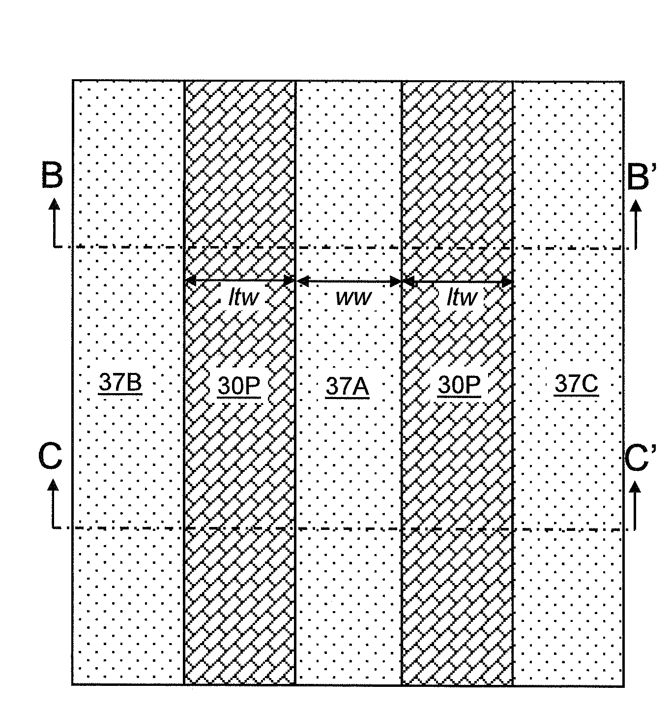
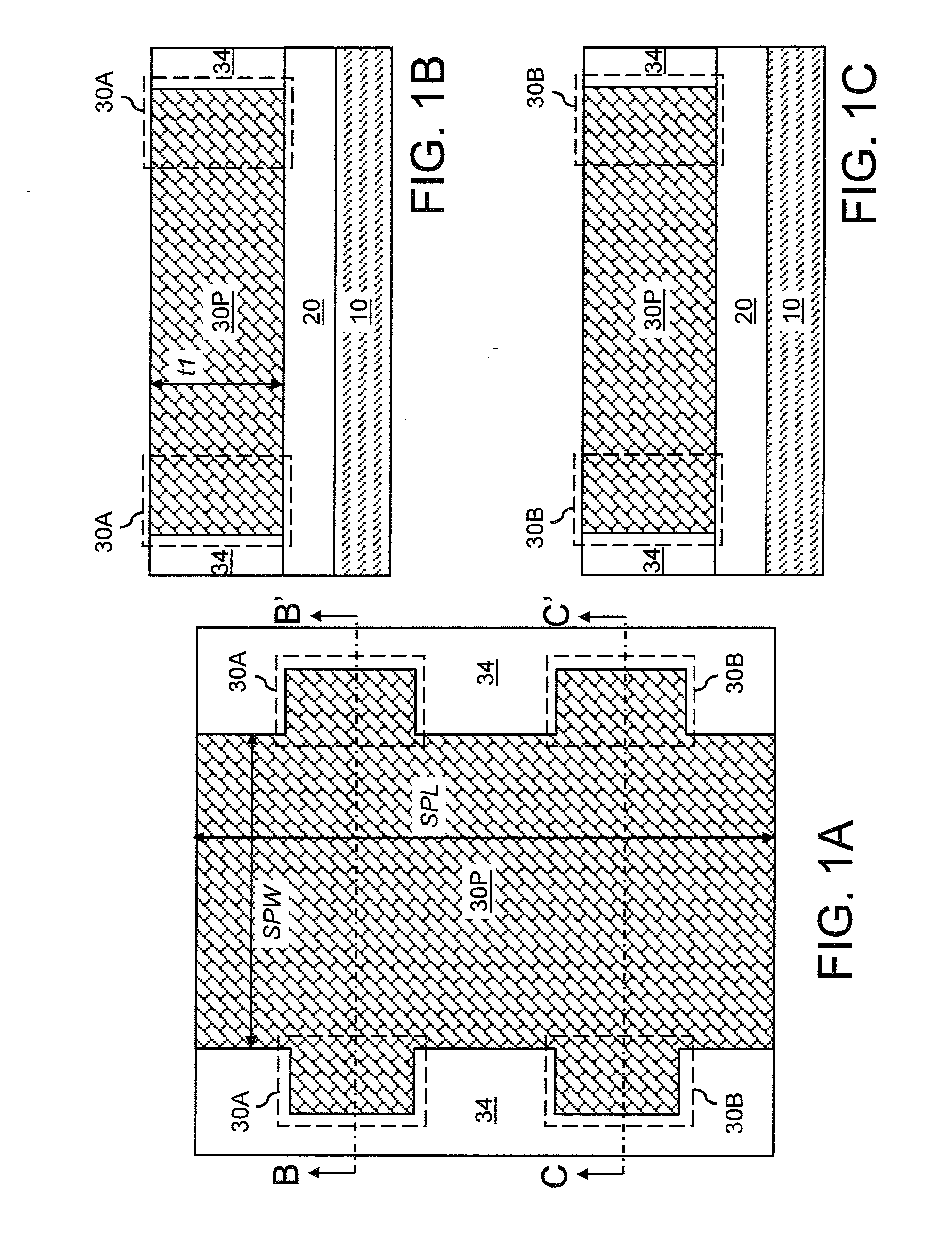
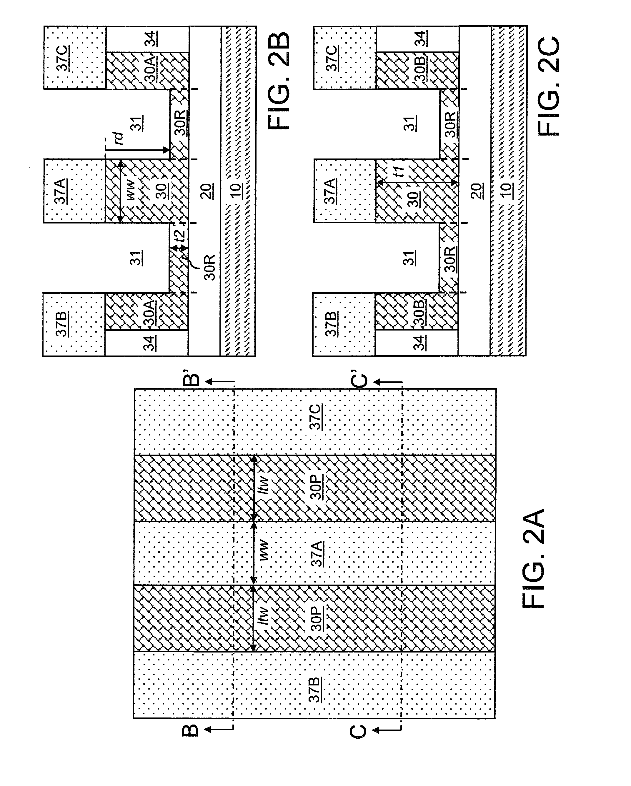
[0124]Referring to FIG. 17, a third exemplary semiconductor structure according to the present invention is derived from the second exemplary semiconductor structure by forming a substantially intrinsic lower semiconductor portion 30 and a substantially intrinsic upper semiconductor portion 138 in each temperature control device. A vertically abutting pair of a substantially intrinsic lower semiconductor portion 30 and a substantially intrinsic upper semiconductor portion 138 is herein referred to as a substantially intrinsic semiconductor portion (30, 138). Thus, each of the at least one temperature control device may include the substantially intrinsic semiconductor portion 30.

[0125]The substantially intrinsic semiconductor portion (30, 138) is formed between a p-doped semiconductor portion (131, 132) and an n-doped semiconductor portion (133, 134) of the at least one temperature control device (90, 142, 131, 132, 140, 30, 138, 133, 134, 144, 92). The substantially intrinsic semic...

fifth embodiment

[0129]Referring to FIG. 19, a fifth exemplary semiconductor structure according to the present invention is derived from the second exemplary semiconductor structure by omitting formation of at least one compound semiconductor via 85.

[0130]Referring to FIG. 20, a sixth exemplary semiconductor structure according to a sixth embodiment of the present invention is derived from the second exemplary semiconductor structure at a step corresponding to FIGS. 14A and 5B by removing the photoresist 147 and employing a non-conformal deposition process to form a low-k dielectric material portion 150. The material of the low-k dielectric material portion 150 may be the same as in the second embodiment. The non-conformal property of the deposition process employed to form the low-k dielectric material portion 150 deposits a low-k dielectric material over narrow portions of the of the semiconductor structures above the top surface of the buried insulator layer 20, i.e., between the at least one te...

seventh embodiment

[0132]Referring to FIG. 22, a seventh exemplary semiconductor structure according to the present invention is shown. FIG. 111 is a top-down view of selected elements including p-doped semiconductor portions (131, 132), n-doped semiconductor portions (133, 134), first metal semiconductor alloy regions 140, second metal semiconductor alloy regions 142, third metal semiconductor alloy regions 144, first metal contact vias 90, second metal contact vias 92, and a semiconductor waveguide 136. The location of the optoelectronic device 160 is shown in a broken line. A vertical cross-sectional view along the plane Z-Z′ is the same as FIG. 15A.

[0133]Each of the first metal semiconductor alloy regions 140 is located within a first annulus. Each of the p-doped semiconductor portions (131, 132) and n-doped semiconductor portions (133, 134) is located within a second annulus which encloses and abuts the first annulus. Each of the second metal semiconductor alloy regions 142 and the third metal se...


PUM


Abstract

Current may be passed through an n-doped semiconductor region, a recessed metal semiconductor alloy portion, and a p-doped semiconductor region so that the diffusion of majority charge carriers in the doped semiconductor regions transfers heat from or into the semiconductor waveguide through Peltier-Seebeck effect. Further, a temperature control device may be configured to include a metal semiconductor alloy region located in proximity to an optoelectronic device, a first semiconductor region having a p-type doping, and a second semiconductor region having an n-type doping. The temperature of the optoelectronic device may thus be controlled to stabilize the performance of the optoelectronic device.

Description

BACKGROUND[0001]The present invention relates to a semiconductor structure, and particularly to a temperature control device for an optoelectronic device and a germanium photodetector for silicon waveguide, and methods of manufacturing the same, and methods of operating the same.[0002]A semiconductor waveguide may be employed in microphotonic devices to enable high efficiency long range transmission of light over distances in the micrometer range or in the millimeter range. The semiconductor waveguide typically employs a single crystalline semiconductor material to minimize signal loss due to absorption of light. The semiconductor material in the semiconductor waveguide has a relative high refractive index. For example, silicon and germanium have a refractive index of about 3.45 and about 4.0, respectively. A dielectric material having a lower refractive constant surrounds the semiconductor waveguide so that a total reflection condition is satisfied at the interface between the semi...

Claims


Application Information

Patent Timeline
IPC IPC(8): H01S3/04G02B6/12H01L21/00
CPCG02B6/12004G02B6/1347H01L35/34G02F1/0147G02F1/025G02B2006/12069H10N10/01
Inventor ASSEFA, SOLOMONGREEN, WILLIAM M.KIM, YOUNG-HEEVAN CAMPENHOUT, JORISVLASOV, YURII A.
Owner GLOBALFOUNDRIES US INC
Why Eureka
Try Eureka