Structure and method to fabricate high performance MTJ devices for spin-transfer torque (STT)-RAM application

a technology of spin-transfer torque and high-performance mtj, which is applied in the direction of magnetic materials for record carriers, instruments, transportation and packaging, etc., can solve the problems of signal error, read process introduces statistical difficulties, and the use of external magnetic fields generated by current carrying lines to switch the magnetic moment direction, etc., and achieves high-density mtj arrays

Active Publication Date: 2011-01-20
TAIWAN SEMICON MFG CO LTD
View PDF13 Cites 134 Cited by
  • Summary
  • Abstract
  • Description
  • Claims
  • Application Information

AI Technical Summary

Benefits of technology

[0027]All of the layers in the MTJ stack may be formed by sputtering or ion beam deposition (IBD). Once all the layers in the MTJ stack are laid down, a thermal anneal process may be employed to fix the pinned layer magnetization (easy-axis) direction. The MTJ stack is patterned with a photo

Problems solved by technology

As the size of MRAM cells decreases, the use of external magnetic fields generated by current carrying lines to switch the magnetic moment direction becomes problematic.
Needless to say, the read process introduces some statistical difficulties associat

Method used


Image

  • Structure and method to fabricate high performance MTJ devices for spin-transfer torque (STT)-RAM application
  • Structure and method to fabricate high performance MTJ devices for spin-transfer torque (STT)-RAM application
  • Structure and method to fabricate high performance MTJ devices for spin-transfer torque (STT)-RAM application

Examples


Embodiment Construction

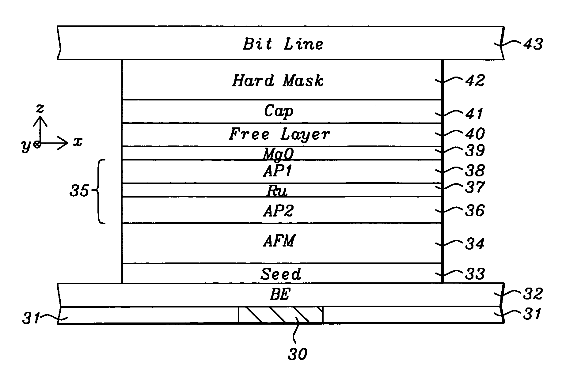
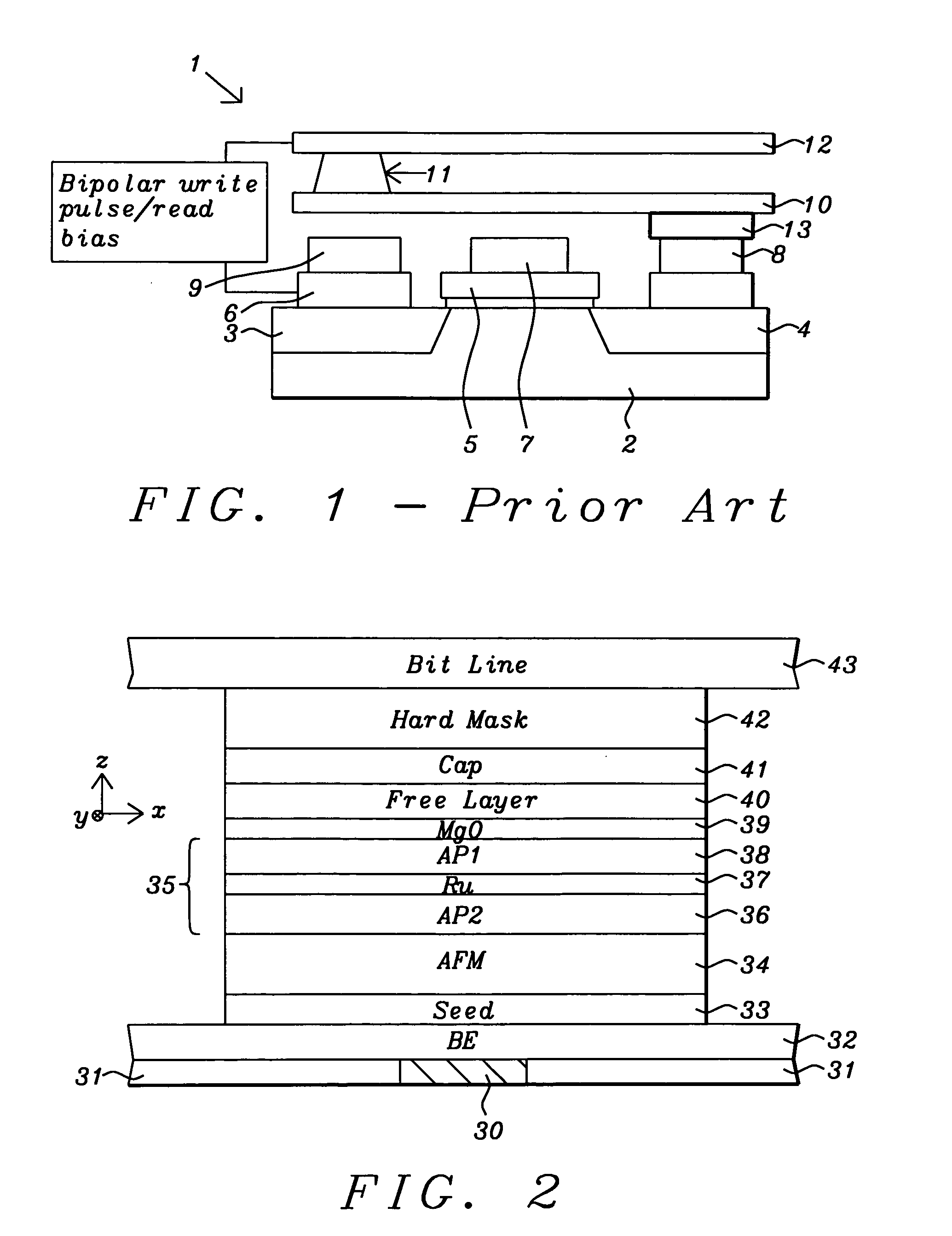
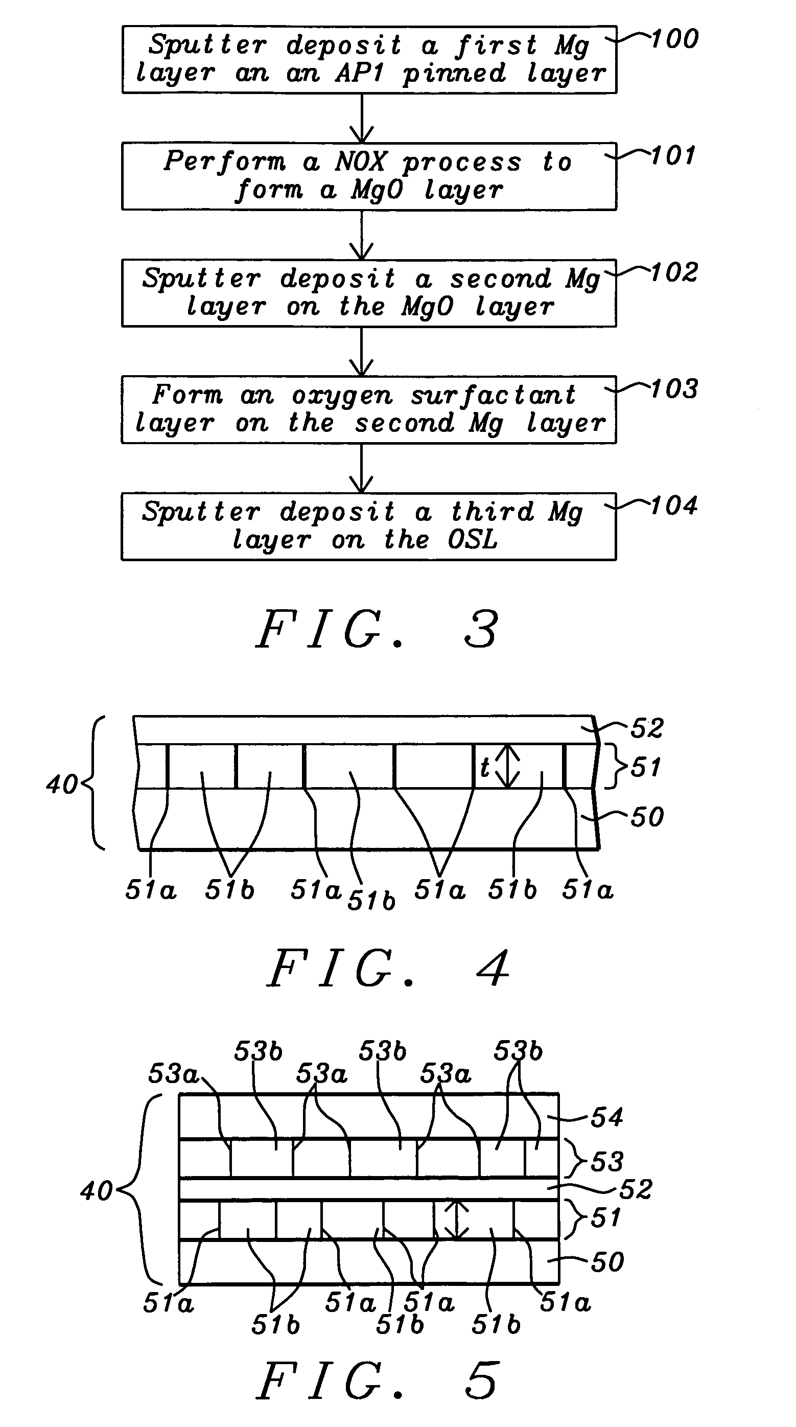
[0039]The present invention is a MTJ element (nanopillar) that provides low JC0 and high thermal stability to enable enhanced performance necessary for advanced devices including 64 Mb STT-RAMs. The present invention also includes a method of forming a MTJ element for an ultra high density STT-RAM device. Although the exemplary embodiment depicts a bottom spin valve configuration, the present invention also encompasses a top spin valve design and dual spin valves as appreciated by those skilled in the art. A “top view” as described herein is defined as a viewpoint from a position above the plane of the substrate in the STT-RAM device. Note that the thicknesses for the magnetic layers and NCC layers in the free layer configuration described in various embodiments are based on a MagIC measurement scale and are thinner than determined by a HR-TEM (high resolution-transmission electron microscopy) measurement. In general, a conversion factor of 1.3 should be applied which means a 13.5 A...


PUM

PropertyMeasurementUnit
Temperatureaaaaaaaaaa
Thicknessaaaaaaaaaa

Abstract

A STT-RAM MTJ is disclosed with a MgO tunnel barrier formed by natural oxidation and containing an oxygen surfactant layer to form a more uniform MgO layer and lower breakdown distribution percent. A CoFeB/NCC/CoFeB composite free layer with a middle nanocurrent channel layer minimizes Jc0 while enabling thermal stability, write voltage, read voltage, and Hc values that satisfy 64 Mb design requirements. The NCC layer has RM grains in an insulator matrix where R is Co, Fe, or Ni, and M is a metal such as Si or Al. NCC thickness is maintained around the minimum RM grain size to avoid RM granules not having sufficient diameter to bridge the distance between upper and lower CoFeB layers. A second NCC layer and third CoFeB layer may be included in the free layer or a second NCC layer may be inserted below the Ru capping layer.

Description

RELATED PATENT APPLICATIONS[0001]This application is related to the following: Docket # HMG08-007, Ser. No. 12 / 284,066, filing date Sep. 18, 2008; which is assigned to a common assignee and is herein incorporated by reference in its entirety.FIELD OF THE INVENTION[0002]The invention relates to a high performance Magnetic Tunneling Junction (MTJ) element and a method for making the same, and in particular, to a spin transfer torque (STT-RAM) device that achieves low switching current and high dR / R by incorporating a free layer having a FL1 / NCC / FL2 configuration in which the nano-conducting channels in the middle NCC layer magnetically and electrically couple the two portions FL1 and FL2 of the free layer.BACKGROUND OF THE INVENTION[0003]Magnetoresistive Random Access Memory (MRAM), based on the integration of silicon CMOS with MTJ technology, is a major emerging technology that is highly competitive with existing semiconductor memories such as SRAM, DRAM, and Flash. Similarly, spin-t...

Claims


Application Information

Patent Timeline
IPC IPC(8): G11B5/706C23C14/34B44C1/22
CPCY10T428/1114H01L43/12B82Y25/00G11C11/16C23C14/3414G11C11/161H10N50/01H10N50/85H10N50/10
Inventor HORNG, CHENG T.TONG, RU-YINGLIU, GUANGLIBEACH, ROBERTKULA, WITOLDMIN, TAI
Owner TAIWAN SEMICON MFG CO LTD
Why Eureka
Try Eureka