MEMS stress concentrating structure for MEMS sensors

a technology of stress concentrating structure and mems sensor, which is applied in the direction of instruments, fluid pressure measurement, loudspeakers, etc., can solve the problems of affecting the performance of the instrument, the inability to compete with the two-chip mems microphone or the ecm microphone, and the parameter functions are often not very well controlled by the manufacturing technology

Active Publication Date: 2011-03-03
KONTEL DATA SYST
View PDF12 Cites 26 Cited by
  • Summary
  • Abstract
  • Description
  • Claims
  • Application Information

AI Technical Summary

Benefits of technology

[0025]With the stress concentrator structure, it is possible to construct different mechanical sensors with relatively simple process steps in a MEMS technology for microphone and pressure sensor.
[0026]In a first aspect, there is provided a plate of monolithic material or composite material having different layers of a predetermined shape. The plate is delineated into an outer region and an inner region by slits, of predetermined shapes, cut into the plate. The outer region is supported on a pedestal and it can be joined as part of the whole to a pedestal or separated from it by a thin film of material. The outer region and the inner region are joined by multiple stress concentrator bridges which are formed when the cuts are made. Each stress concentrator bridge acts to concentrate or amplify the stress in the stress concentrator bridges caused by point or distributed forces acting on the inner region or part of the inner region. The stress concentrator bridges may have but do not need to have the same composition of material layers as the inner region.

Problems solved by technology

These parameters are often not very well controlled functions of a manufacturing technology.
For these reasons the cost of the single chip MEMS microphone remains high and is unable to compete with the two chip MEMS microphone or the ECM microphone.
The two imperfections must be controlled and contribute to the complexity of the design and affects the manufacturing yield of a capacitive MEMS microphone.
Silicon rich nitride has a lower stress but because its oxidation leads to silicon oxynitride which is difficult to etch, its use within the IC production process is not mainstream and often avoided.
Since oxide and nitride are not conductors, polysilicon is often used as material for the conducting plates in conjunction with nitride or oxide because polysilicon must be protected from the environment due to its richness in grain boundaries, which can lead to point of weakness when the material is exposed to etchants.
The stress from such composites is even harder to control.
Such growth, however, takes place at an elevated temperature (usually >900° C.) and as to be seen later, may not be a desirable part of the capacitive sensor formation process unless the sensor plates are formed as part of the IC process itself.
If true, this will compromise and introduce variations to the basic IC process which adds significant cost and complexity to the already complicated IC process.
The thickness control using these methods ranges from fair to poor.
The surface tension in a small droplet of water would pull the two surfaces together during drying and the surface atomic force can keep the surface attached, therefore destroying the function of the sensor.
Since aqueous processing is an essential part of the MEMS manufacturing as well as a cutting process to eliminate silicon particle contamination, stiction places serious constraints on the realization of capacitive sensing structures and post-process fabrication steps.
But use of the latter is not possible during wafer cutting, adding a further complication to the manufacturing process.
To avoid melting the metallic aluminum interconnect, the processing temperature must be kept below 450° C. This places constraints on the choice of materials that can be used for the mechanical structures, conducting or non-conducting, their properties and the methods of deposition.
Even if some of these layers and steps can be shared with the basic IC process, the process is still a relatively complicated endeavor.
Not many combinations of materials are available as solutions.
They are often very complex.
The circuit is small by VLSI standards but its size is not linearly scalable with respect to technology line-width shrinkage.
In general, the noise of the capacitive MEMS microphone is limited by kT / C noise where C is the capacitance of the MEMS sensor and parasitic capacitances.
A common fallacy in designing capacitive microphone is the assumption that with decreasing C, the sensitivity can be restored by making the flexible plate thinner.
But such an act would decrease the maximum voltage at which the sensor can operate due to the decreasing pull-in voltage of the electrostatic attraction, thus negating any improvement that comes from making the capacitor thinner.
The disadvantages of the plate / piezoresistive structure are that it is extremely hard to control the uniformity and thickness of a large plate during the etching process.
A non-uniformity of the plate causes errors in the reading of the piezoresistor.
It further limits the size of a pressure sensor in that a minimal force has to be created through the area of the plate to create a detectable stress.

Method used


Image

  • MEMS stress concentrating structure for MEMS sensors
  • MEMS stress concentrating structure for MEMS sensors
  • MEMS stress concentrating structure for MEMS sensors

Examples


Embodiment Construction

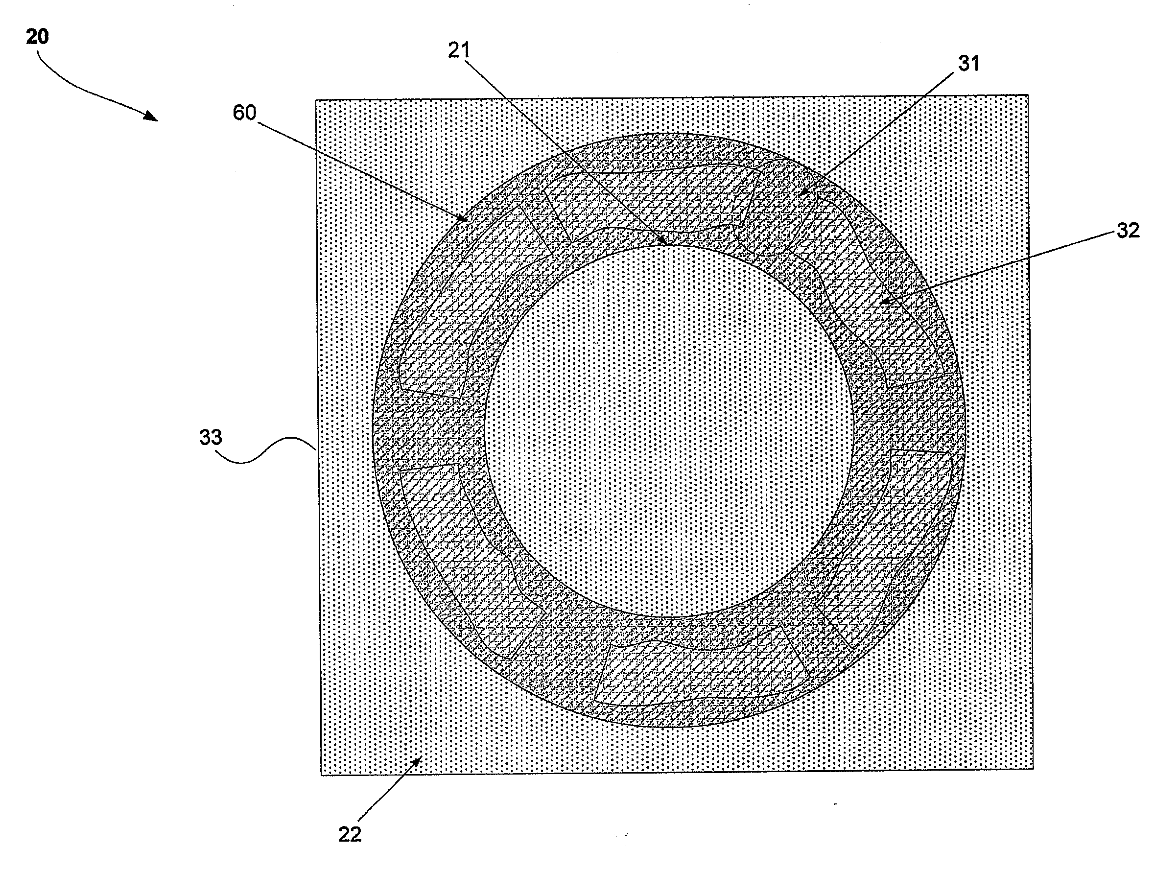
[0052]FIG. 3 shows the construction of a MEMS stress concentrator structure 20. The structure 20 includes a plate 33, usually having a rectangular outer boundary. The plate 33 can be formed by a single monolithic material or multi-layers of different materials as depicted in FIG. 4. The plate 33 has an outer region 22 and inner region 21 which is defined by slits 32 formed in the plate 33 by photolithographic patterning and etching. The slits 32 can be of any predetermined shape to suit the MEMS sensor design and accommodate internal stresses in the inner region 21 as well as stresses from external forces. The usual lateral dimension are on the order of tens to hundreds of microns. The width of the inner region 21 can range from a fraction of a millimeter to several millimeters. The inner region 21 is part of the plate 33. But the inner region 21 does not have to have the same thickness or vertical composition as the outer region 22. The inner region 21 can be altered in its vertica...


PUM

PropertyMeasurementUnit
pressureaaaaaaaaaa
temperatureaaaaaaaaaa
noise voltageaaaaaaaaaa

Abstract

A stress concentrating apparatus and a method for a MicroElectroMechanical System (MEMS) sensors is provided. The apparatus includes a plate having an inner region and outer region, the inner region being separated from the outer region by slits defined in the plate. A stress concentrator bridge connects the inner region to the outer region, and to mechanically amplify stress applied on the inner region of the plate. At least one stress sensor is operatively connected to the stress concentrator bridge, whereby the at least one stress sensor converts the mechanically amplified stress applied on the inner region into an electrical signal.

Description

[0001]This nonprovisional application claims priority to U.S. Provisional Application No. 61 / 239,068, which was filed on Sep. 2, 2009, and which is herein incorporated by reference.BACKGROUND OF THE INVENTION[0002]1. Field of the Invention[0003]The invention relates to a design for and methods for the manufacturing of a stress concentrating structure for applications in MicroElectroMechanical System (MEMS) sensors in particular with respect to microphone and pressure sensor involving the entire or partial composition of all electronic and mechanical elements of the device functions on a silicon substrate or any other material.[0004]2. Description of the Background Art[0005]Smaller size, better performance and lower cost per function are the major driving forces behind the modern electronic industries. To achieve such goals, the industry is attempting to integrate more functions, including mechanical sensors and their sensing electronics, into miniaturized chips.[0006]The most common...

Claims


Application Information

Patent Timeline
Patent Type & Authority Applications(United States)
IPC IPC(8): G01L9/06C23F1/00H04R31/00
CPCG01L9/0054H04R23/006Y10T29/49002B81B3/0086G01L9/0042B81B2201/0264Y10T29/42H04R2201/003H04R17/00H04R31/00B81B2201/0257
Inventor LI, PING WAI
Owner KONTEL DATA SYST
Why Eureka
Try Eureka