Thin film transistor manufacturing method, thin film transistor, thin film transistor substrate and image display apparatus, image display apparatus and semiconductor device

a technology of thin film transistors and manufacturing methods, applied in static indicating devices, instruments, vacuum evaporation coatings, etc., can solve the problems of difficult film forming, large amount of energy and an increased number of steps, and difficulty in reducing the number of masks or the like, etc., to achieve the speed of film forming, the effect of improving the mobility and on-off ratio, and improving the time required for film forming

Inactive Publication Date: 2011-03-03
IDEMITSU KOSAN CO LTD
View PDF8 Cites 112 Cited by
  • Summary
  • Abstract
  • Description
  • Claims
  • Application Information

AI Technical Summary

Benefits of technology

[0167]FIG. 5 is a schematic view showing the state in which a channel layer is formed by the method for producing a thin film transistor according to the first embodiment of the present invention, in which (a) is a cross-sectional view showing the state in which an amorphous oxide film is formed, (b) is a cross-sectional view showing the state in which the amorphous oxide film is patterned, and (c) is a cross-sectional view showing the state in which the amorphous oxide film is crystallized and a channel layer composed of the crystalline oxide film is formed.
[0168]In FIG. 5(a), in the above-mentioned step of forming a channel layer (S1-3), an amorphous oxide film 1001a is formed at first (S1-3-1).
[0169]The thickness of this amorphous oxide film 1001a is normally about 0.5 to 500 nm, preferably about 1 to 150 nm, more preferably about 3 to 80 nm, and particularly preferably about 10 to 60 nm. This is because it will become difficult to form a film uniformly on the industrial base if the thickness is smaller than about 0.5 nm. On the other hand, if the thickness is larger than about 500 nm, the time required for film forming is too long to be industrially implemented. On the other hand, if the thickness is within the range of about 3 to 80 nm, the TFT characteristics including the mobility and the on-o...

Problems solved by technology

Moreover, since a high temperature of 800° C. or more is needed to attain crystallization, for example, it is difficult to form a crystalline silicon-based thin film on a glass substrate and an organic substance substrate.
Moreover, a large amount of energy and an increased number of steps are needed in manufacturing.
Furthermore, in the case of a TFT using a crystalline silicon-based thin film, it is normally restricted to have a top gate-type configuration.
Therefore, cost reduction by reducing the number of masks or the like is usually difficult.
Therefore, an amorphous silicon semiconductor may not be effective to display a high-speed animation when used as a switching element for driving an image display unit.
Furthermore, when irradiated with visible light, this semiconductor active l...

Method used


Image

  • Thin film transistor manufacturing method, thin film transistor, thin film transistor substrate and image display apparatus, image display apparatus and semiconductor device
  • Thin film transistor manufacturing method, thin film transistor, thin film transistor substrate and image display apparatus, image display apparatus and semiconductor device
  • Thin film transistor manufacturing method, thin film transistor, thin film transistor substrate and image display apparatus, image display apparatus and semiconductor device

Examples


example 1

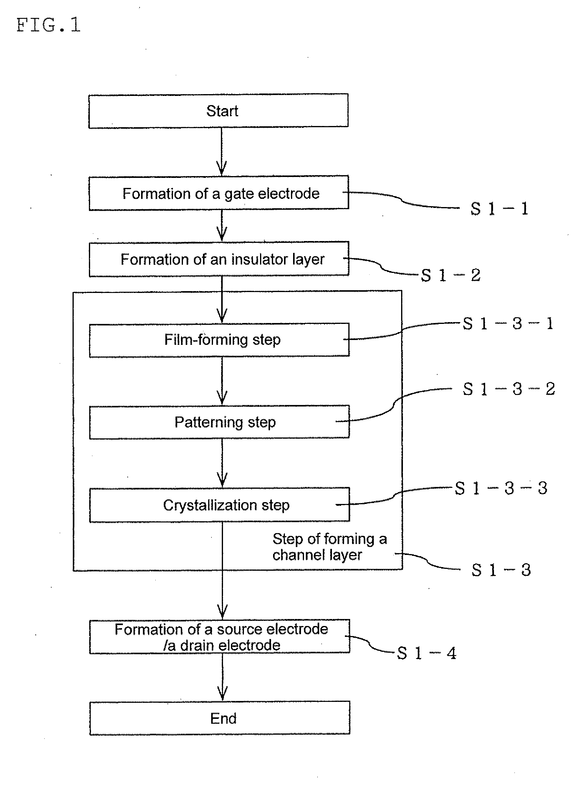
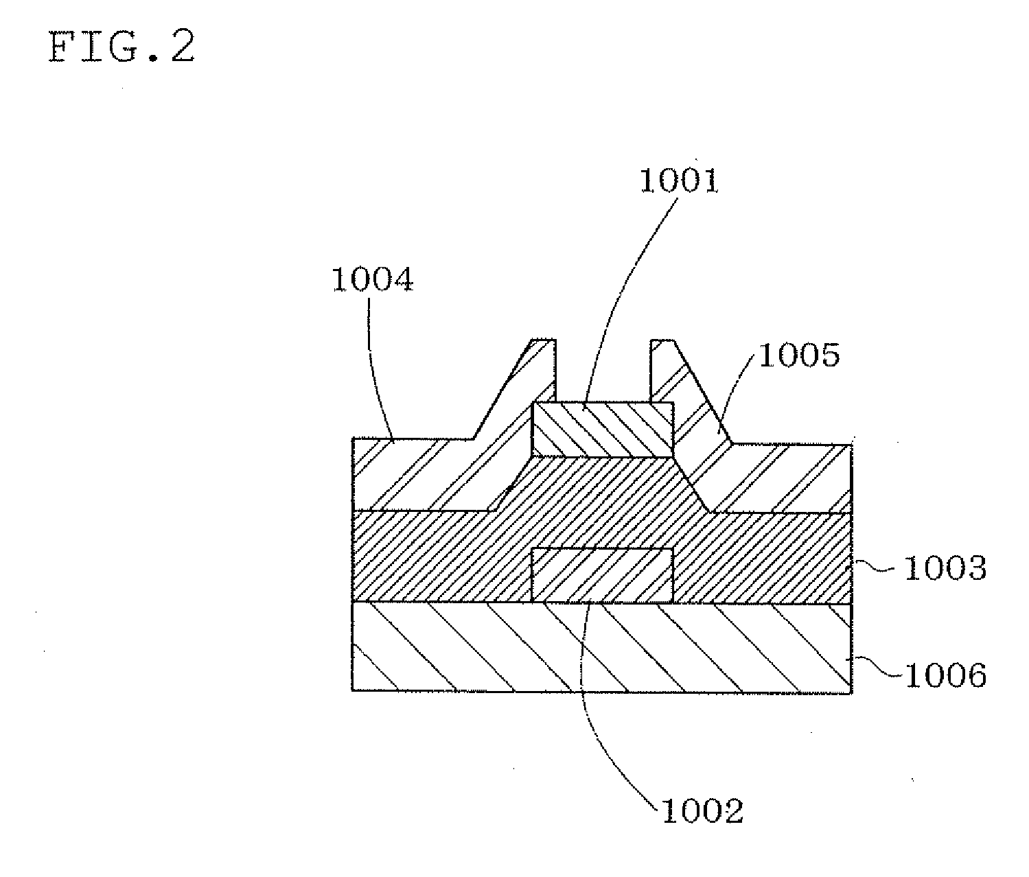
[0222]In this example, an inverted-staggered type thin film transistor shown in FIG. 2 was manufactured according to the process shown in FIG. 1.

(1) Non-alkaline glass (Corning 1737 glass, manufactured by Corning Inc.) was used as a substrate 1006 (see FIG. 3 (a)).

(2) Mo was formed into a film of 200 nm by the DC magnetron sputtering method as a conductive film 1002a (see FIG. 3(b)).

(3) The conductive film 1002a was patterned by the photolithography using a PAN etching solution (40° C.), whereby a gate electrode 1002 was formed (see FIG. 3(c), S1-1).

(4) SiNx was formed as a gate-insulating film by the CVD method, whereby an insulator film 1003 was formed (see FIG. 4, S1-2).

(5) An In2O3—ZnO sputtering target (atomic ratio [In / (In+Zn)]=0.93, atomic ratio [Zn / (In+Zn)]=0.07) and the glass substrate 1006 obtained in (4) above were installed in the film-forming equipment of the DC magnetron sputtering method, which is one of the DC sputtering methods, and a film was formed. The sputtering...

example 2

[0225]The method for producing a thin film transistor in this example was substantially the same as that in Example 1, except that, in the sputtering in (5), an In2O3—ZnO sputtering target (atomic ratio [In / (In+Zn)]=0.98, atomic ratio [Zn / (In+Zn)]=0.02) was used.

[0226]The thin film transistor produced by the method as mentioned above had a channel width L of 100 μm, the channel length W of 500 μm, and a W / L of 5. This thin film transistor exhibited the field-effect mobility of 35 (cm2 / Vs), 104 or more of an on-off ratio and normally-off properties.

[0227]An electron microscopic observation after the etching with an oxalic acid etching solution in (6) above revealed that a slight amount of etching residues remained.

[0228]In addition, 20 thin film transistors were manufactured by the same method as mentioned above. It was found that 17 of them operated normally, while 3 did not operate.

example 3

[0229]The method for producing a thin film transistor in this example was substantially the same as that in Example 2, except that the atmospheric gas used in the sputtering in (5) composed of 99 vol % of Ar and 1 vol % of H2O.

[0230]The thin film transistor produced by the method as mentioned above had a channel width L of 100 μm, the channel length W of 500 μm, and a W / L of 5. This thin film transistor exhibited a field-effect mobility of 35 (cm2 / Vs), 106 or more of an on-off ratio and normally-off properties.

[0231]An electron microscopic observation after the etching with an oxalic acid etching solution in (6) above revealed that almost no etching residues remained.

[0232]In addition, 20 thin film transistors were manufactured by the same method as mentioned above. It was found that all 20 transistors operated normally.


PUM

PropertyMeasurementUnit
Temperatureaaaaaaaaaa
Fractionaaaaaaaaaa

Abstract

To provide a method for producing a thin film transistor improved in stability, uniformity, reproducibility, heat resistance, durability or the like, a thin film transistor, a thin film transistor substrate, an image display apparatus, an image display apparatus and a semiconductor device.
In the semiconductor device, a crystalline oxide is used as an N-type transistor and the electron carrier concentration of the crystalline oxide is less than 2×10¹⁷/cm3. Furthermore, the crystalline oxide is a polycrystalline oxide containing In and one or more positive divalent elements selected from Zn, Mg, Cu, Ni, Co and Ca, and the atomic ratio In [In] and the positive divalent element [X][X]/([X]+[In]) is 0.0001 to 0.13.

Description

TECHNICAL FIELD[0001]The present invention relates to a method for producing a thin film transistor, a thin film transistor produced by this production method, a thin film transistor substrate on which this thin film transistor is arranged, and an image display apparatus using this thin film transistor. In the method for producing a thin film transistor, an amorphous oxide film is formed as a channel layer, the amorphous oxide film is patterned and then crystallized, and the thus crystallized crystalline oxide film is a channel layer.[0002]Furthermore, the present invention relates to an image display apparatus in which a crystalline oxide having a prescribed electron carrier concentration is used as an active layer of a field-effect type transistor.[0003]Furthermore, the present invention relates to a semiconductor device, in particular, to a semiconductor device in which a crystalline oxide having a prescribed electron carrier concentration is used as an N-type semiconductor.BACKG...

Claims


Application Information

Patent Timeline
IPC IPC(8): G09G5/10
CPCC23C14/086C23C14/3414H01L21/02554H01L29/66969H01L21/02631H01L29/7869H01L21/02565
Inventor YANO, KOKIINOUE, KAZUYOSHIUTSUNO, FUTOSHIKASAMI, MASASHI
Owner IDEMITSU KOSAN CO LTD
Why Eureka
Try Eureka