Manufacturing method of planar optical waveguide device with grating structure

a technology of planar optical waveguide and grating structure, which is applied in the direction of photomechanical equipment, instruments, originals for photomechanical treatment, etc., can solve the problems of large amount of power consumed by a computer system or a high-end router, economic efficiency but also environmental impact, and the price of the optical component will drop in the future. , to achieve the effect of easy and precise formation, low cost and reduced length

Active Publication Date: 2011-03-03
ADVANCED MICRO FOUNDRY PTE LTD
View PDF5 Cites 15 Cited by
  • Summary
  • Abstract
  • Description
  • Claims
  • Application Information

AI Technical Summary

Benefits of technology

[0032]According to the above-described manufacturing method of the planar optical waveguide device, the polarization independent waveguide structure can be realized by forming a groove in the upper or lower portion of the core. In addition, the groove can be easily and precisely formed in the core by the step of filling both the sides after forming the groove section filler.
[0033]Compared with the known chirped grating in which the pitch changes gradually, the length can be reduced for miniaturization while realizing high functionality and the processing accuracy can be easily controlled in the manufacturing process.
[0034]Since the grating optical waveguide is designed by solving the inverse scattering problem using the Zakharov-Shabat equations, the planar optical waveguide device having an optical characteristic of a complicated function, such as the chromatic dispersion compensator which compensates the group delay dispersion and the dispersion slope of optical fiber transmission lines simultaneously over a number of DWDM channels, can be made small with a short waveguide length.
[0035]Since the planar optical waveguide device can be manufactured by the silicon photonics technology in which the CMOS manufacturing process is used, mass production becomes possible. As a result, the price of the device can be reduced. In addition, the device can be made small by adopting the high relative refractive index difference optical waveguide structure.
[0036]As a result of having designed the grating optical waveguide by solving the inverse scattering problem using the Zakharov-Shabat equations, the pitch in the grating optical waveguide takes a plurality of certain discrete values and the core width of the optical waveguide and the lateral width of the grooved structure are not uniform. Since the grating pitch takes a plurality of certain discrete values, process control becomes easier unlike with the chirped type.
[0037]When the grating structure is formed, the first exposure step of forming shaded portions on the photoresist layer using the phase-shifting photomask and the lateral width of the shaded portions at positions corresponding to the fin portions are extended and wider than the designed values of respective core widths of the fin portions and exposing the photoresist layer at the outside of said shaded portions, and the second exposure step of forming shaded portions on the photoresist layer using the binary-type photomask and the lateral widths of the shaded portions at positions corresponding to the fin portions are substantially equal to the designed values of respective core widths of the fin portions, are adopted. Accordingly, even if the old exposure apparatus which uses light with a wavelength of 248 nm is used, a grating optical waveguide having a complicated shape can be manufactured as designed.

Problems solved by technology

On the other hand, as the sizes of information communication systems and the number of information communication systems installed increase rapidly, the large amount of power consumed by a computer system or a high-end router becomes a problem from the points of view of not only economic efficiency but also environmental impact.
Moreover, since it is a manufacturing process suitable for mass production, it is expected that the price of the optical component will drop in the future.
However, in the Fiber Bragg Grating, there is a limitation on the range where the refractive index can be changed to form the grating pattern.
Accordingly, knowledge on the photolithography process using a photomask has not been sufficiently accumulated yet.
For this reason, when the surrounding structures are formed, a case often occurs where the latest fine process cannot necessarily be applied and the old technology node, such as thick-film resist application, needs to be used.

Method used


Image

  • Manufacturing method of planar optical waveguide device with grating structure
  • Manufacturing method of planar optical waveguide device with grating structure
  • Manufacturing method of planar optical waveguide device with grating structure

Examples


first embodiment

of a Planar Optical Waveguide Device

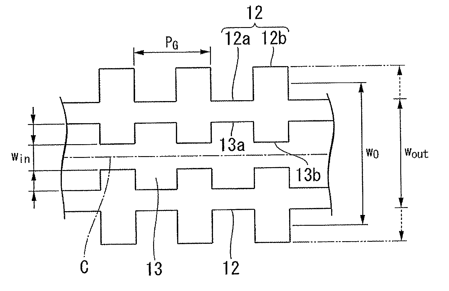
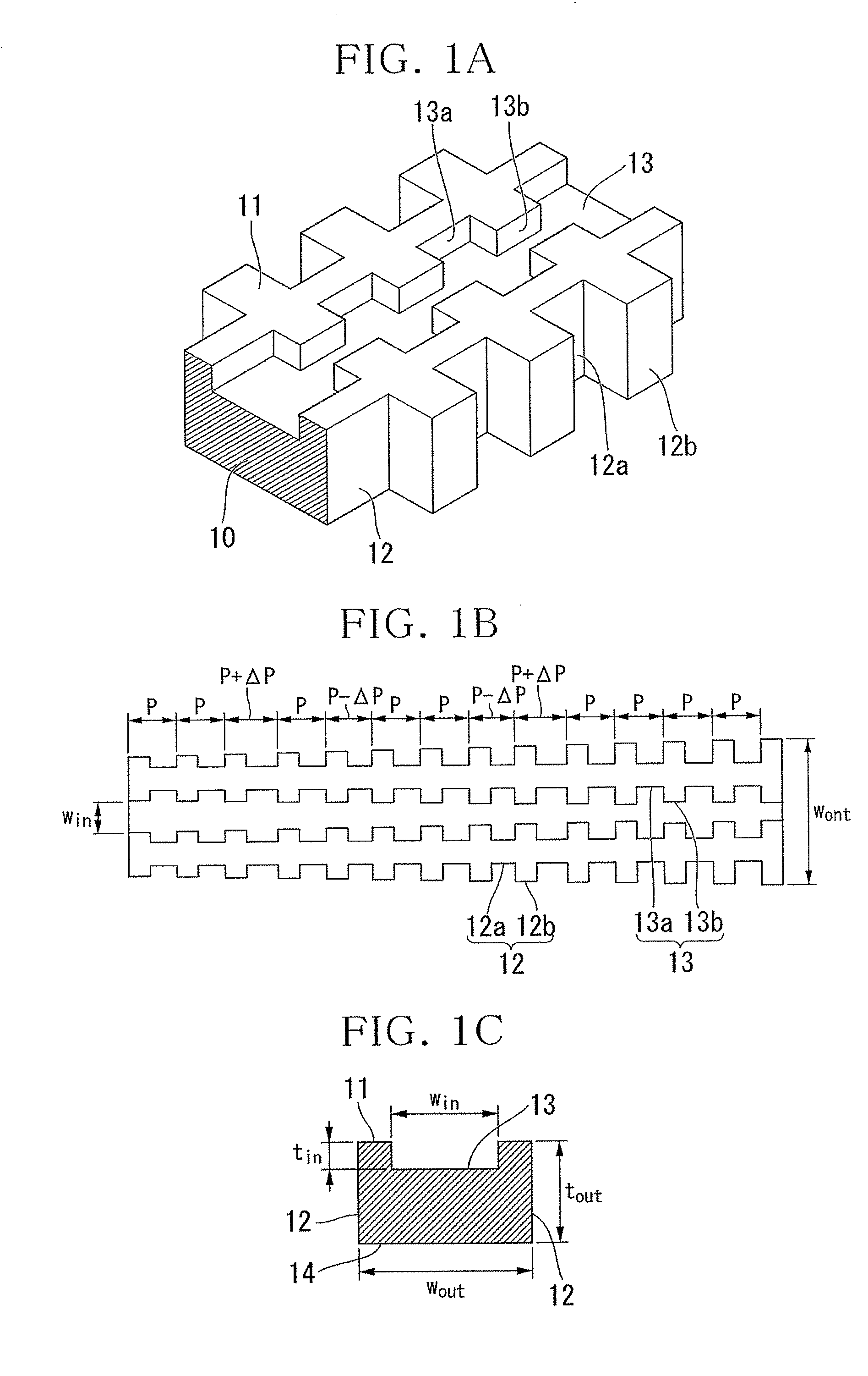
[0156]A planar optical waveguide device according to a first embodiment of the present invention is schematically shown in FIGS. 1A to 1C. FIG. 1A is a perspective view illustrating a part of a core 10 of an optical waveguide, FIG. 1B is a top view illustrating the same part of the core 10, and FIG. 1C is a cross-sectional view illustrating the planar optical waveguide device. In addition, a perspective view of the planar optical waveguide device is shown in FIG. 16. In the meantime, in FIG. 1C, reference numerals 12 and 13 are used to denote a sidewall and a grooved structure of the core 10 without distinguishing valleys (valley portions) 12a and 13a and fins (fin portions) 12b and 13b of FIGS. 1A and 1B.

[0157]In this planar optical waveguide device the optical waveguide is formed on a substrate 15. The optical waveguide has a lower cladding 16 formed on the substrate 15, the core 10 formed on the lower cladding 16, and an upper cladding 17 forme...

first example

[0260]As shown in FIGS. 1A to 1C, the chromatic dispersion compensator of the polarization independent planar optical waveguide in which the core was formed of silicon nitride (SiN) and the cladding was formed of silica glass (SiO2) and which had the grating structure on the sidewall and upper portion of the core of the optical waveguide was designed and manufactured.

[0261]The cross-sectional structure of the optical waveguide was designed according to the structure of FIG. 1C, and the correlation of win and wout with the effective refractive index of the optical waveguide was calculated as shown in FIG. 5.

[0262]Then, the grating pattern was designed. The designed center frequency was 188.4 THz. That is, the designed center wavelength was 1591.255 nm. The group delay dispersion and dispersion slope of the single-mode dispersion shifted fiber (DSF) with a length of 100 km which is specified in ITU-T G.653 with a channel interval of 100 GHz in L-Band and over 45 channels in the channe...

second embodiment

of the Planar Optical Waveguide Device

[0285]FIG. 35 is a perspective view illustrating a planar optical waveguide device according to a second embodiment of the present invention.

[0286]The planar optical waveguide device has a grating structure 112 on a sidewall of an optical waveguide core 110 and a grooved grating structure 113 on a bottom surface 114 of the core 110. A top surface 111 of the core 110 is flat. The optical waveguide has a lower cladding 116 formed on a substrate 115, the core 110 formed on the lower cladding 116, and an upper cladding 117 formed on the core 110 and the lower cladding 116.

[0287]In the present embodiment, the same grooved grating structure 13 as the grooved grating structure 113, which is configured to include the fin 13b and the valley 13a in the first embodiment, is formed in a bottom portion of the core 110. The grooved grating structure 113 has a fin (fin portions) 113b and a valley (valley portions) 113a formed on both sides of the groove.

(Manuf...


PUM

PropertyMeasurementUnit
wavelengthaaaaaaaaaa

Abstract

A method for manufacturing a planar optical waveguide device including a core of which a top face is provided with a groove section filled with a groove section filler made of a low refractive index material having a refractive index lower than that of the core, the method including; a first high refractive index material layer forming step of forming a high refractive index material layer; a low refractive index material layer forming step of forming a low refractive index material layer made of the low refractive index material on the high refractive index material layer; a groove section filler forming step of forming the groove section filler by trimming both lateral portions of the low refractive index material layer; and a second high refractive index material layer forming step of forming a high refractive index material layer so as to fill the both sides of the lateral portions of the groove section filler.

Description

TECHNICAL FIELD[0001]The present invention relates to a manufacturing method of a planar optical waveguide device with a grating structure.BACKGROUND ART[0002]In recent years, the amount of information transmitted through the optical fiber communication network has rapidly increased due to the progress in the optical fiber communication system, especially due to the invention of the erbium-doped fiber amplifier (EDFA) and the dense wavelength division multiplexing (DWDM) system. In order to meet the demand for increased data capacity, research and development to increase the number of wavelengths to be multiplexed is being carried out on a modulation method in which the frequency efficiency is high. In the DWDM system, there is a need for an optical component having a more advanced function, such as a chromatic dispersion compensator which compensates the wavelength dispersion and the dispersion slope of each channel more precisely than the dispersion compensation optical fiber modu...

Claims


Application Information

Patent Timeline
Patent Type & Authority Applications(United States)
IPC IPC(8): G03F7/20
CPCG02B6/124G02B6/136G02B6/132
Inventor SAKUMA, KENOGAWA, KENSUKEGOI, KAZUHIROTAN, YONG TSONGGUAN, NINGYU, MINGBINTEO, HWEE GEELO, GUO-QIANG
Owner ADVANCED MICRO FOUNDRY PTE LTD
Why Eureka
Try Eureka