Semiconductor device and method for manufacturing semiconductor device

Active Publication Date: 2011-07-21
SUMITOMO ELECTRIC IND LTD
View PDF8 Cites 0 Cited by
  • Summary
  • Abstract
  • Description
  • Claims
  • Application Information

AI Technical Summary

Benefits of technology

[0008]The methods disclosed in Patent Literatures 1 and 2 lead to significantly satisfactory results on a p-type GaN on the c-plane of a GaN substrate. According to the inventor's knowledge, a satisfactory ohmic electrode, however, cannot be formed on a p-type GaN on a non-polar or a semipolar GaN substrate, probably due to a thick surface oxide film peculiar to a not-polar surface (the surface is not polar). A difference in the effect of oxide films results from a difference in state (Ga—O bond) of the surface oxide

Problems solved by technology

According to the inventor's knowledge, a satisfactory ohmic electrode, however, cannot be formed on a p-type GaN on a non-polar or a semipolar GaN substrate, probably due to a thick surface oxide film peculiar to a not-pola

Method used


Image

  • Semiconductor device and method for manufacturing semiconductor device
  • Semiconductor device and method for manufacturing semiconductor device
  • Semiconductor device and method for manufacturing semiconductor device

Examples


Example

Example 1

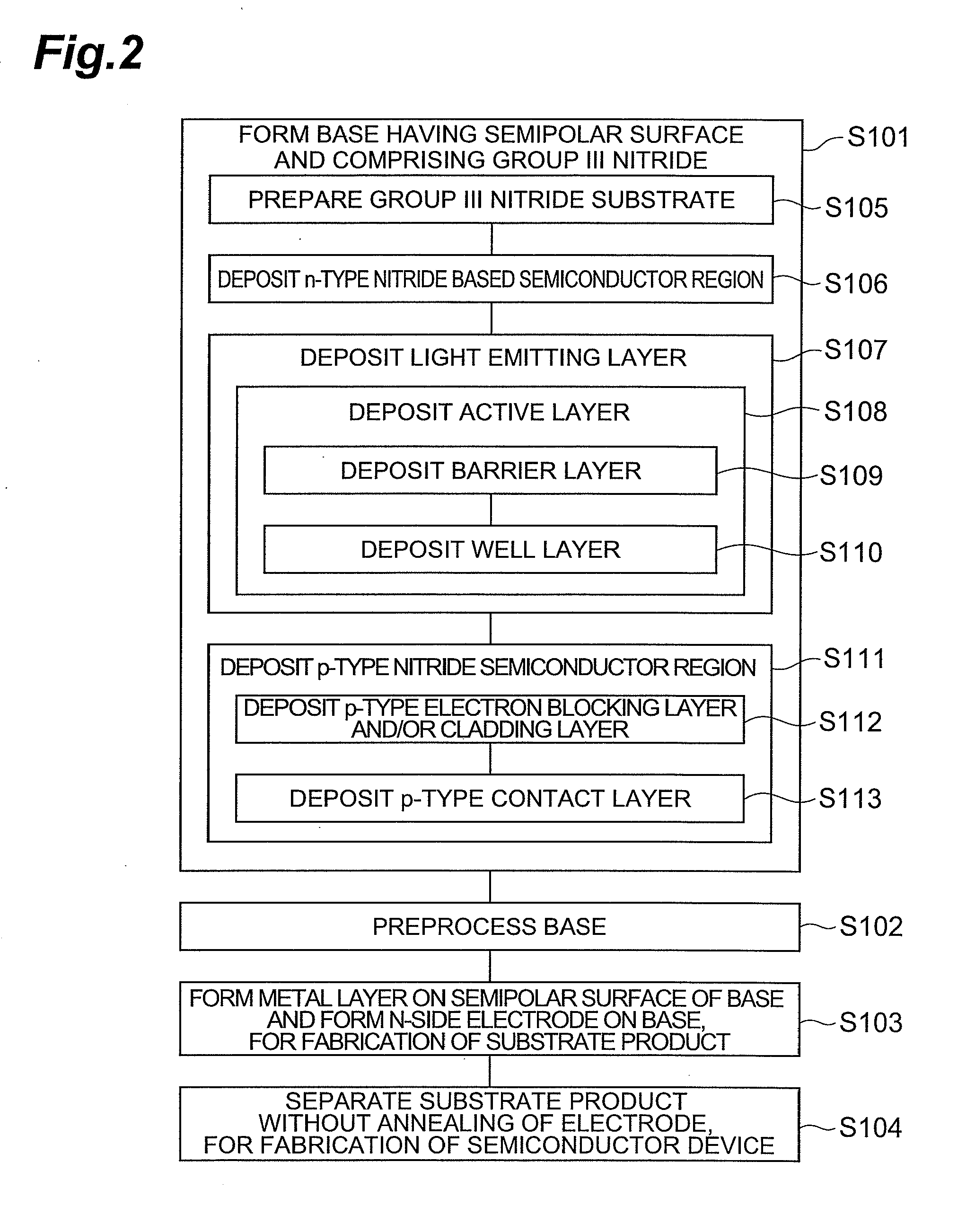
[0059]An epitaxial substrate having a structure shown in Part (a) of FIG. 3 is made by metalorganic chemical vapor deposition (MOCVD). A GaN buffer layer may be deposited, if necessary, on a semipolar surface having a c-axis tilting toward an m-axis of an n-type GaN substrate by MOCVD. Subsequently, an n-type GaN layer doped with silicium having a thickness of 1 μm, a p-type GaN layer doped with magnesium having a thickness of 0.4 μm, and p+-type GaN layer heavily doped with magnesium having a thickness of 50 nm are deposited.

[0060]Prior to the deposition of a p-type electrode film, a circular resist is formed by photolithography. Subsequently, in the same deposition system, a platinum film having a thickness of 50 nm and a Ni / Au film having a thickness of 5 nm / 11 nm are deposited by electron beam evaporation and resistive heating, respectively. The degree of vacuum is about 1×10⁻⁶ Torr.

[0061]After the deposition, the resist is lifted off in acetone to form platinum electro...

Example

Example 2

[0065]The interface between GaN and an electrode is analyzed by X-ray photoelectron spectroscopy (XPS). An epitaxial substrate with a surface of c-plane (device A for evaluation) and a semipolar epitaxial substrate (device B for evaluation) are deposited by epitaxy as in Example 1. A platinum electrode is deposited by electron beam evaporation on each of these epitaxial substrates (devices A and B) to form a substrate product with a surface of c-plane (device C for evaluation) and a semipolar substrate product (device D for evaluation). In addition, a Ni / Au film is deposited on each of these epitaxial substrates (devices A and B) by electron beam evaporation and then resistive heating to form a substrate product with a surface of c-plane (device E for evaluation) and a semipolar substrate product (device F for evaluation).

[0066]In the manufacturing process of all the devices for evaluation, the epitaxial substrates are subjected to the organic cleaning and acid cleaning pri...

Example

Example 3

[0070]In order to confirm the dependence of semipolar characteristics on the tilt angle, four semipolar substrates having a tilt angle of +5 degrees, −5 degrees, +10 degrees, and −10 degrees, respectively, from the (20-21) plane, and a not-polar substrate with a surface of m-plane are prepared. Epitaxial substrates are made by using these GaN substrates as in Example 2. The epitaxial substrates are analyzed by using the XPS as in Example 2. The results demonstrate that non-alloy platinum electrode formed on an epitaxial substrate using a semipolar or non-polar GaN substrate has a superior interface to an alloy electrode on a c-plane. Within the range of the tilt angle, no significant difference is observed in electrical properties measured. Consequently, a non-alloy electrode formed on a substrate having a not-polar (i.e. semipolar or non-polar) principal surface having different characteristics from a polar c-plane has satisfactory ohmic characteristics.

[0071]As described ...


PUM


Abstract

A semiconductor device has a satisfactory ohmic contact on a p-type principal surface tilting from a c-plane. The principal surface 13a of a p-type semiconductor region 13 extends along a plane tilting from a c-axis (axis <0001>) of hexagonal group-III nitride. A metal layer 15 is deposited on the principal surface 13a of the p-type semiconductor region 13. The metal layer 15 and the p-type semiconductor region 13 are separated by an interface 17 such that the metal layer functions as a non-alloy electrode. Since the hexagonal group-III nitride contains gallium as a group-III element, the principal surface 13a comprising the hexagonal group-III nitride is more susceptible to oxidation compared to the c-plane of the hexagonal group-III nitride. The interface 17 avoids an increase in amount of oxide after the formation of the metal layer 15 for the electrode.

Description

BACKGROUND OF THE INVENTION[0001]1. Field of the Invention[0002]The present invention relates to a semiconductor device and a method for manufacturing the semiconductor device.[0003]2. Related Background Art[0004]Patent Literature 1 (Japanese Unexamined Patent Application Publication No. 05-291621) discloses an ohmic contact to a c-plane of a layer using a metal such as Ag or Ni on GaxAl1-xN doped with a p-type impurity. After the deposition of a metal layer, annealing is performed in an oxygen atmosphere. A high intensity light-emitting device having a low driving voltage is thereby produced using a gallium nitride-based semiconductor.[0005]Patent Literature 2 (Japanese Unexamined Patent Application Publication No. 09-64337) discloses an ohmic contact of a c-plane to a p-type layer. A nickel layer is formed on a surface of p+ layer, and a gold layer is formed on the nickel layer. Subsequently, through heat treatment, the distribution of the elements in depth direction is inverted. ...

Claims


Application Information

Patent Timeline
IPC IPC(8): H01L29/45H01L21/02
CPCH01L33/16H01L33/40H01L33/32H01L33/36
Inventor TOKUYAMA, SHINJIADACHI, MASAHIROKYONO, TAKASHISAITO, YOSHIHIRO
Owner SUMITOMO ELECTRIC IND LTD
Why Eureka
Try Eureka