Organic semiconducting compositions and n-type semiconductor devices

a semiconductor and composition technology, applied in the direction of naphthalimide/phthalimide dyes, non-metal conductors, conductors, etc., can solve the problems of amorphous silicon application limitation to low-speed devices, requiring relatively costly processes, and amorphous silicon application is limited to low-speed devices, so as to enhance the operational stability of the device, improve the control of the morphology of the thin film, and improve the control of the semiconductor film morph

Active Publication Date: 2011-07-28
EASTMAN KODAK CO
View PDF22 Cites 24 Cited by
  • Summary
  • Abstract
  • Description
  • Claims
  • Application Information

AI Technical Summary

Benefits of technology

[0040]The presence of certain polymeric additives that have a permittivity of at least 1.5 and up to and including 5 provides better control over thin film morphology and enhances operational stability of OFET devices comprising such an inventive layer. The addition of a polymer in coating...

Problems solved by technology

Application of amorphous silicon is limited to low speed devices, however, since its maximum mobility (0.5-1.0 cm2/V·sec) is about a thousand times smaller than that of crystalline silicon.
The deposition of amorphous silicon, during the manufacture of transistors, requires relatively costly processes, such as plasma enhanced chemical vapor deposition and high temperatures (about 360° C.) to achieve the electrical characteristics sufficient for display applications.
Such high processing temperatures disallow the use of substrates, for deposition, made of certain plastics that might otherwise be desirable for use in applications such as flexible displays.
One such naphthalene-based n-channel semiconductor material, tetracyanonaphthoquino-dimethane (TCNNQD), is capable of operation in air, but the material has displayed a low on/off ratio and is also difficult to prepare and purify.
In crystalline organic films defects, like grain boundaries and disorder inside the grains, are limiting factors for the mobility and the diffusion length of the charge carriers.
Unfortunately, some deposition techniques that are more amenable to manufacturing do not readily permit slow evaporation of solvent.
For example, though spin coating can yield relatively uniform thin films, the solvent usually leaves the film relatively quickly, generally leading to a low degree of crystal order.
Other manufact...

Method used


Image

  • Organic semiconducting compositions and n-type semiconductor devices
  • Organic semiconducting compositions and n-type semiconductor devices
  • Organic semiconducting compositions and n-type semiconductor devices

Examples


invention example 1

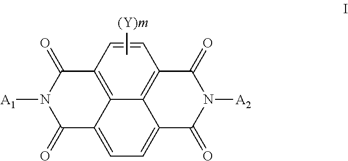
[0177]A heavily doped silicon wafer with a thermally-grown SiO2 layer with a thickness of 195 nm was used as the substrate. The wafer was cleaned for 10 minutes in a piranha cleaning solution, followed by a 6-minute exposure in a UV / ozone chamber. An organic semiconducting formulation consisting essentially of N,N′-trans-4-pentylcyclohexyl)-1,4,5,8-naphthodiimide (Compound I-4) (0.5 weight %) and polystyrene (0.5 weight %, Aldrich Chemical Co., average Mw 200,000) in distilled 1,2,4-trimethylbenzene was coated onto silicon dioxide dielectric at 800 RPM for 30 seconds followed by 5000 RPM for 45 seconds. A sample was annealed in air at 100° C. for 1 hour. Subsequently, a gold source and drain electrodes were vapor deposited through a shadow mask to a thickness of 50 nm. The resulting devices had a 650 μm channel width, with channel lengths varying from 50 to 150 μm. Multiple OFET's were prepared and 4 to 12 representative samples were tested for each deposition run. The averaged resu...

invention example 2

[0185]An organic semiconducting formulation consisting essentially of N,N′-trans-4-pentylcyclohexyl)-1,4,5,8-naphthodiimide (Compound I-4) (0.5 weight %) and polystyrene (0.5 weight %, Aldrich Chemical Co., average Mw 200,000) as the polymer additive in distilled 1,2,4-trimethylbenzene was coated onto the PMMA dielectric layer at 800 RPM for 30 seconds followed by 5000 RPM for 45 seconds. Each sample was annealed in air at 100° C. for 1 hour. Subsequently, a gold source and drain electrodes were vapor deposited through a shadow mask to a thickness of 50 nm. The resulting devices had a 650 μm channel width with channel lengths varying from 50 to 150 μm. Multiple OFET's were prepared and 4 to 12 representative samples were tested for each deposition run. The averaged results appear in TABLE II below.

[0186]The electrical parameters of the devices were measured and calculated as described for Invention Example 1. The average mobility was found to be 0.64 cm2 / V·sec in the saturation regi...

invention example 3

[0189]An organic semiconducting layer formulation consisting essentially of N,N′-trans-4-pentylcyclohexyl)-1,4,5,8-naphthodiimide (Compound I-4) (0.5 weight %) and Zeonex® RS420 (0.1 weight %) in distilled 1,2,4-trimethylbenzene was coated onto the PMMA dielectric layer at 800 RPM for 30 seconds followed by 5000 RPM for 45 seconds. Each sample was annealed in air at 100° C. for 1 hour. Subsequently, a gold source and drain electrodes were vapor deposited through a shadow mask to a thickness of 50 nm. The resulting devices had a 650 μm channel width with channel lengths varying from 50 to 150 μm. Multiple OFET's were prepared and 4 to 12 representative samples were tested for each deposition run. The averaged results appear in TABLE III below along with the results previously reported for Test Device 3 (Comparative Example 2).

[0190]The electrical parameters of the devices were measured and calculated as described above for Invention Example 1. The average mobility was found to be 0.7...


PUM


Abstract

An organic semiconducting composition consists essentially of an N,N-dicycloalkyl-substituted naphthalene diimide and a polymer additive comprising an insulating or semiconducting polymer having a permittivity at 1000 Hz of at least 1.5 and up to and including 5. This composition can be used to provide a semiconducting layer in a thin-film transistor that can be incorporated into a variety of electronic devices.

Description

FIELD OF THE INVENTION[0001]The present invention relates to the use of certain N,N′-dicycloalkyl-substituted naphthalene diimide compounds with polymeric additives in organic semiconducting layers and compositions that can be used in various n-type electronic devices such as thin film transistors and integrated circuits.BACKGROUND OF THE INVENTION[0002]Thin film transistors (“TFT's”) are widely used as switching elements in electronics, for example, in active-matrix liquid-crystal displays, smart cards, and a variety of other electronic devices and components thereof. The thin film transistor (TFT) is an example of a field effect transistor (“FET”). The best-known example of an FET is the “MOSFET (Metal-Oxide-Semiconductor-FET) that can be used for high-speed applications. Most thin film devices are made using amorphous silicon as the semiconductor because amorphous silicon is a less expensive alternative to crystalline silicon. This fact is especially important for reducing the co...

Claims


Application Information

Patent Timeline
IPC IPC(8): H01L51/00H01B1/12
CPCH01L51/0053H01L51/0541Y02E10/549H01L51/0566H01L51/0545C09B57/08H10K85/621H10K10/488H10K10/464H10K10/466
Inventor SHUKLA, DEEPAKMEYER, DIANNE M.
Owner EASTMAN KODAK CO
Why Eureka
Try Eureka