Electromagnetic wave absorbent material

a technology of electromagnetic waves and absorbent materials, applied in the field of transparent electromagnetic wave absorbent materials, can solve the problems of increasing the risk of unnecessary electromagnetic wave radiation and associated interference, the inability to apply to further downsize and integration-increasing mobile instruments, and the serious problem of electromagnetic wave interference inside the instruments. it is easy to achieve the effect of high electromagnetic wave absorption effect, low cost and enabling precision control of magnetic properties

Inactive Publication Date: 2011-07-28
NAT INST FOR MATERIALS SCI
View PDF6 Cites 13 Cited by
  • Summary
  • Abstract
  • Description
  • Claims
  • Application Information

AI Technical Summary

Benefits of technology

[0020]The first invention has made it possible to develop an electromagnetic wave absorbent material taking advantage of the visible light transparency that a transparent magnetic substance has, and has made it possible to produce such an electromagnetic wave absorbent material from a safe, titanium oxide-based material at a low cost.
[0021]Further, the second invention has made it possible to produce a material which utilizes a titania nanosheet having two-dimensional anisotropy, which therefore expresses magnetic resonance in a high-frequency region owing to the magnetic anisotropy caused by the morphology anisotropy thereof, and which exhibits a high electromagnetic wave absorption effect in a GHz band.
[0022]Further, the third invention further has enabled precision control of the magnetic properties of the titania nanosheet and has therefore enabled production of a material having a high electromagnetic wave absorption effect in a GHz band and flexible control of the properties of the material.
[0023]The fourth invention has realized in a simple manner with accuracy a magnetic film comprising a titania nanosheet, and has enabled its use as an electromagnetic wave absorbent device with various materials such as electromagnetic wave absorbent composite sheet, glass, semiconductor device and the like, favorable for application to various mobile electronic instruments such as mobile telephones, wireless LANs, etc.
[0024]Further, the fifth invention has made it possible to plan and produce a high-quality electromagnetic wave absorbent film comprising a titania nanosheet, for devices having the intended thickness and electromagnetic wave absorption properties.
[0025]The sixth invention has provided a further accurate and high-quality magnetic film where a titania nanosheet and a binder are multilayered, and has realized an electromagnetic wave absorbent device excellent in electromagnetic wave absorbability.

Problems solved by technology

In that manner, a lot of electromagnetic wave generation sources surround us, and with diversification of the application mode of electromagnetic waves in a high-frequency band, as combined with down-sizing, speeding-up and body-thinning of communication devices, the risk of unnecessary electromagnetic wave radiation and associated interference, malfunction and insufficiency of electronic parts is considered to increase markedly.
In particular, in mobile electronic instruments such as notebook-size computers, mobile telephones and others, with the tendency toward higher frequency, higher density and higher integration of electronic devices, the electromagnetic wave interference inside the instruments is a serious problem; and it is now an important issue to remove the conductive noise in the GHz band that is superimposed as high harmonics on signals of a hundred to hundreds of MHz.
However, the electromagnetic wave absorbent material heretofore developed must have a thickness of at least from 0.05 to 0.1 mm or so for fully exhibiting the performance, and is therefore difficult to apply to further down-sized and integration-increased mobile instruments.
In addition, existing ferrite-based electromagnetic wave absorbent materials could absorb electromagnetic waves only in a specific narrow frequency region, depending on the chemical composition of the powder and the thickness of the radiowave absorber; and those with versatility broadly applicable to different frequency bands are not as yet developed.
Further, with the recent rapid development of mobile telephones, wireless LANs and other mobile electronic instruments, radio interference brings about problems in various sites in medical practice, airliners, etc.

Method used


Image

  • Electromagnetic wave absorbent material
  • Electromagnetic wave absorbent material
  • Electromagnetic wave absorbent material

Examples


example 1

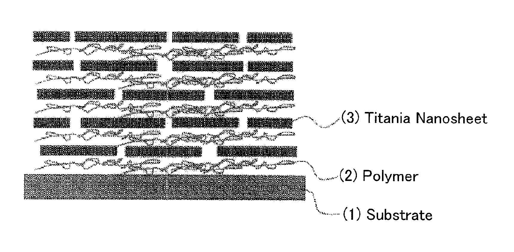
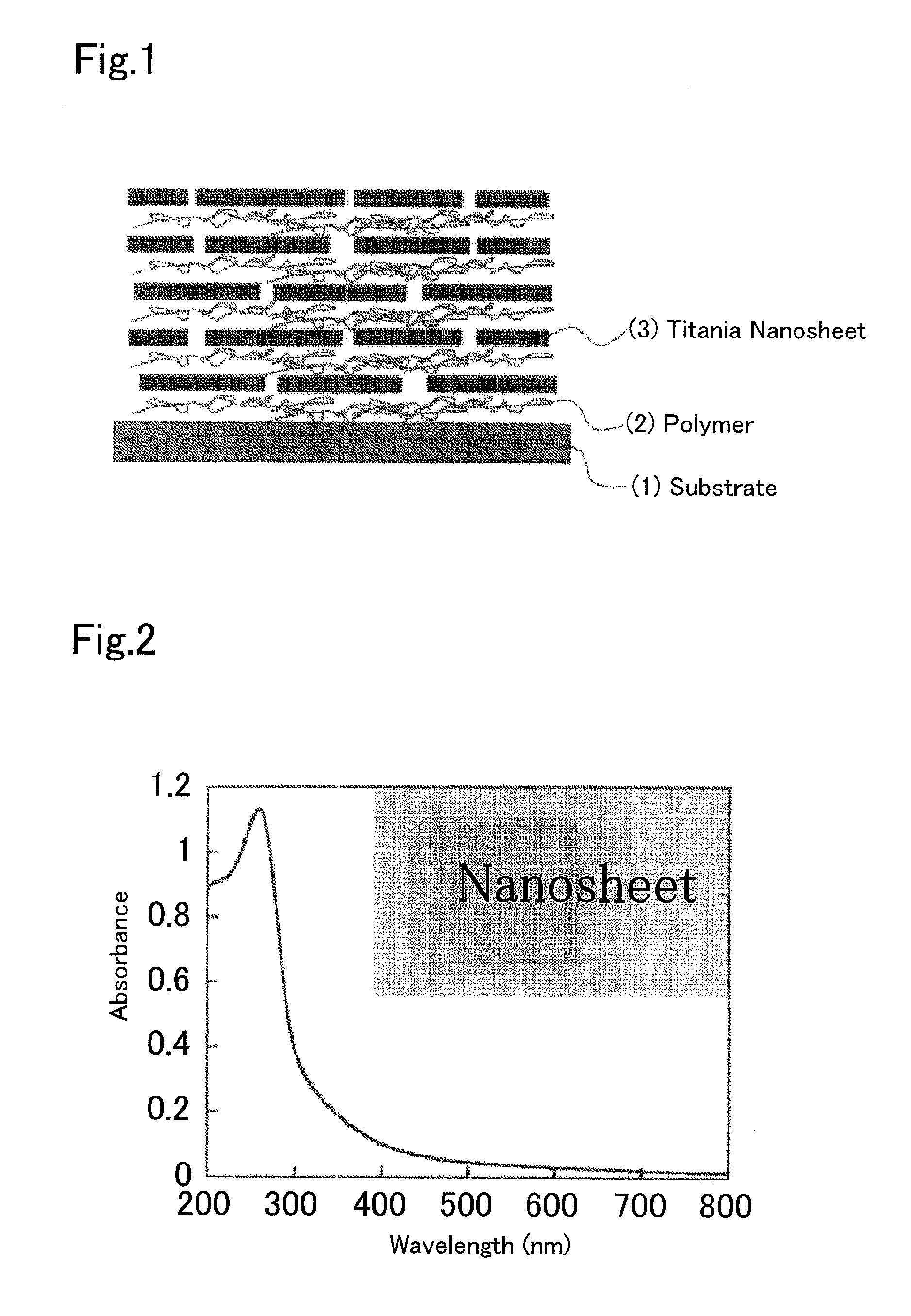
[0060]In this Example, starting from a phyllo-structured titanium oxide (for example, K0.4Ti0.8Co0.2O2), a transparent magnetic substance (3) comprising titania nanosheets (Ti0.8Co0.2O2) is formed, and as shown in FIG. 1, the titania nanosheets (3) and a cationic polymer (2) polydiallyldimethylammonium chloride (PDDA) are alternately laminated on a quartz glass substrate (1) to form a magnetic film thereon in the manner mentioned below, thereby producing an electromagnetic wave absorbent film.

[0061]Phyllo-structured titanium oxide (K0.4Ti0.8Co0.2O2) was prepared by mixing potassium carbonate (K2CO3), titanium oxide (TiO2) and cobalt oxide (CoO) in a ratio K / Ti / Co of 4 / 4 / 1, and then firing it at 800° C. for 40 hours.

[0062]One g of the powder was acid-treated in 100 mL of aqueous 1 N hydrochloric acid solution at room temperature to give a hydrogen-exchanged form (H0.4Ti0.8Co0.2O2). Next, 100 mL of an aqueous solution of tetrabutylammonium hydroxide (hereinafter this is referred to as...

example 2

[0072]In this Example, starting from a phyllo-structured titanium oxide (K0.4Ti0.75Co0.15Fe0.1O2) in which Co and Fe were substituted at the titanium lattice position, a transparent magnetic film comprising titania nanosheets (Ti0.75Co0.15Fe0.1O2) was formed, thereby producing an electromagnetic wave absorbent film of the above-mentioned titania nanosheets (3) and a binder (2) PDDA alternately laminated on a quartz substrate.

[0073]Phyllo-structured titanium oxide (K0.4Ti0.75Co0.15Fe0.1O2) was prepared by mixing potassium carbonate (K2CO3), titanium oxide (TiO2), cobalt oxide (CoO) and iron oxide (Fe2O3) in a ratio K / Ti / Co / Fe of 0.8 / 0.75 / 0.15 / 0.1, and then firing it at 800° C. for 40 hours.

[0074]One g of the powder was acid-treated in 100 mL of aqueous 1 N hydrochloric acid solution at room temperature to give a hydrogen-exchanged form (H0.4Ti0.75Co0.15Fe0.1O2). Next, 100 mL of an aqueous TBAOH solution was added to 0.5 g of the hydrogen-exchanged form and reacted with stirring at ro...

example 3

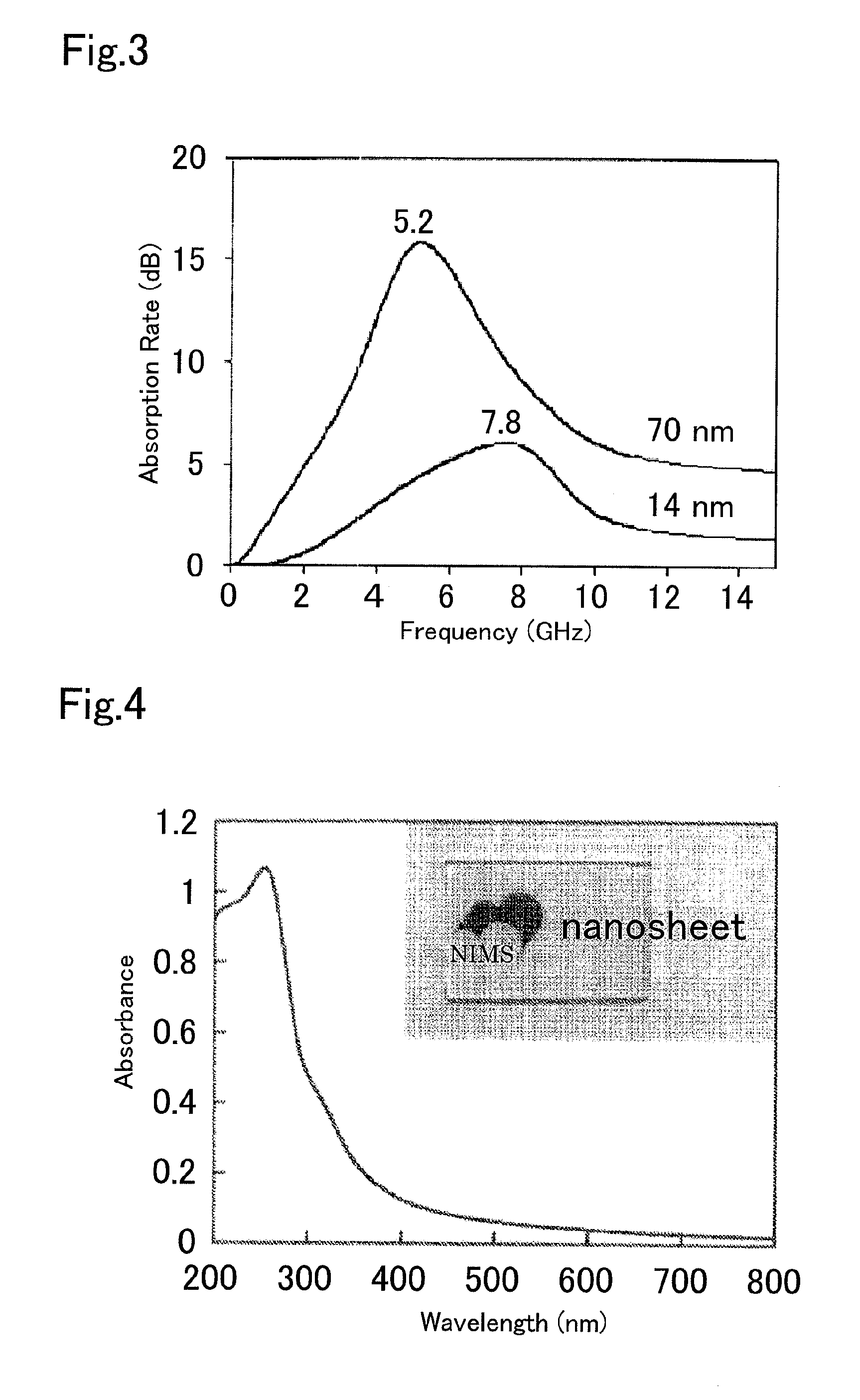
[0080]In this Example, the transparent magnetic substance comprising the titania nanosheets (Ti0.75Co0.15Fe0.1O2) produced in Example 2 was used, and according to a spin coating method, an electromagnetic wave absorbent film having a thickness of a few gill was produced.

[0081]Starting from phyllo-structured titanium oxide (K0.4Ti0.75Co0.15Fe0.1O2) where Co and Fe were substituted at the titanium lattice position, and according to the same method as in Example 2, a sol solution of, as dispersed therein, rectangular nanosheets (2) represented by a compositional formula Ti0.75Co0.15Fe0.1O2 and having a thickness of about 1 nm and a lateral size of from 1 to 10 μm was produced.

[0082]Next, 20 mL of a spin-coating gelatin dispersant was added to 100 mL of the nanosheet dispersion, and stirred at room temperature to prepare a nanosheet solution.

[0083]Using the nanosheet mixture solution and repeating a series of operations mentioned below as one cycle, for a total of the necessary cycles, ...


PUM

PropertyMeasurementUnit
thicknessaaaaaaaaaa
noise frequencyaaaaaaaaaa
thicknessaaaaaaaaaa

Abstract

Provided is an electromagnetic wave absorbent material comprising a magnetic film as the main constituent thereof. The magnetic film comprises a titania nanosheet where a 3d magnetic metal element is substituted at the titanium lattice position. The electromagnetic wave absorbent material stably and continuously exhibits electromagnetic wave absorption performance in a range of from 1 to 15 GHz band and is useful as mobile telephones, wireless LANs and other mobile electronic instruments. The absorbent material can be fused with a transparent medium and is applicable to transparent electronic devices such as large-sized liquid crystal TVs, electronic papers, etc.

Description

TECHNICAL FIELD [0001]The present invention relates to a transparent electromagnetic wave absorbent material which is applied to a broad field of information communication technology such as mobile telephones, wireless LANs, mobile electronic instruments and others and which exhibits favorable electromagnetic wave absorption performance.Background Art[0002]Heretofore, electromagnetic waves are utilized in broadcasts, radars, ship communications, microwave ovens, etc.; and recently, with the noticeable development of information communication technology, their applications have become dramatically expanded. Above all, application of electromagnetic waves in the GHz band level that enable large-capacity information transmission is increasing abruptly, and such electromagnetic waves have become used in mobile telephones (1.5 GHz), ETC systems (5.8 GHz), satellite broadcasting (12 GHz), wireless LANs (2.45 to 60.0 GHz), in-car radars for preventing rear-end collision (76 GHz), etc.[0003...

Claims


Application Information

Patent Timeline
Patent Type & Authority Applications(United States)
IPC IPC(8): B32B9/00B32B5/00H01F1/01
CPCB82Y25/00Y10T428/265C01G23/005C01G45/006C01G51/006C01G53/006C01P2002/52C01P2002/84C01P2004/24C01P2006/42C04B35/462C04B2235/3201C04B2235/3272C04B2235/3275H01F10/007H05K9/0088H05K9/0096H01F10/193C01G23/003
Inventor OSADA, MINORUSASAKI, TAKAYOSHI
Owner NAT INST FOR MATERIALS SCI
Why Eureka
Try Eureka