Hardmask composition for forming resist underlayer film, process for producing a semiconductor integrated circuit device, and semiconductor integrated circuit device

Inactive Publication Date: 2011-10-06
CHEIL IND INC
View PDF5 Cites 8 Cited by
  • Summary
  • Abstract
  • Description
  • Claims
  • Application Information

AI Technical Summary

Problems solved by technology

However, if a photoresist is too thin, difficulty in performing a role as a mask in a subsequent pattern transfer (i.e. etching) process

Method used


Image

  • Hardmask composition for forming resist underlayer film, process for producing a semiconductor integrated circuit device, and semiconductor integrated circuit device
  • Hardmask composition for forming resist underlayer film, process for producing a semiconductor integrated circuit device, and semiconductor integrated circuit device

Examples


example 1

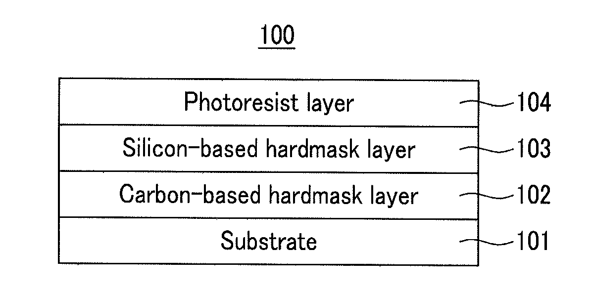
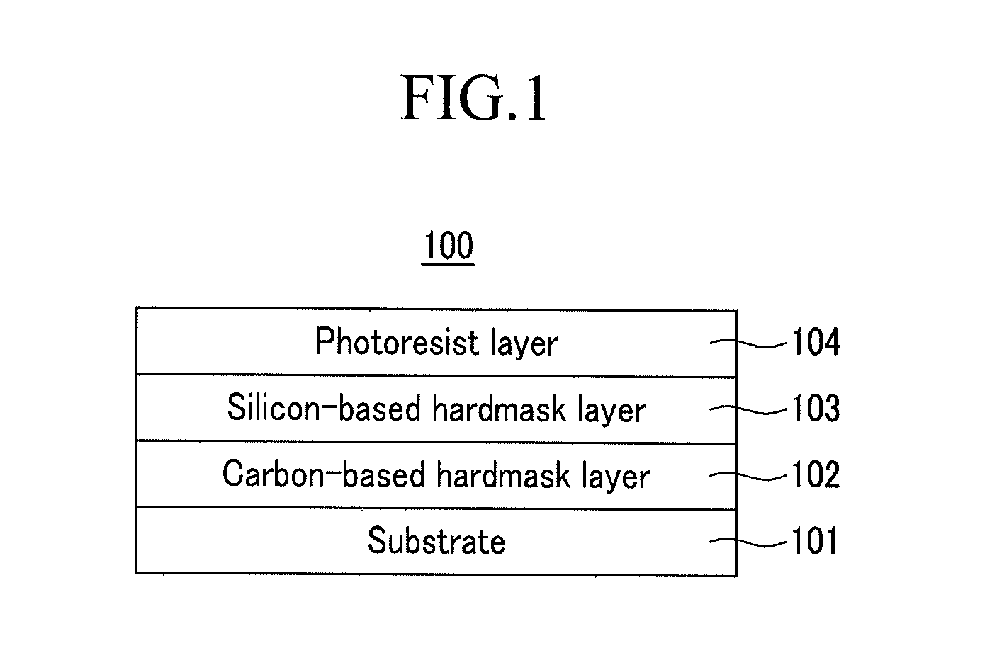
[0096]1,750 g of methyltrimethoxysilane, 340 g of phenyltrimethoxysilane, and 313 g of trimethoxysilane were dissolved in 5,600 g of propylene glycol monomethyl ether acetate (PGMEA) in a 10-liter four-neck flask equipped with a mechanical agitator, a condenser, a dropping funnel, and a nitrogen inlet tube. To the solution was added 925 g of an aqueous nitric acid solution (1,000 ppm). After the mixture was allowed to react at 60° C. for 1 hour, methanol was removed from the reaction mixture under reduced pressure. The reaction was continued for 1 week while maintaining the reaction temperature at 50° C. After completion of the reaction, hexane was added to the reaction mixture to precipitate a polymer.

[0097]2.0 g of the polymer was diluted with 100 g of MIBK, and 0.002 g of pyridinium p-toluenesulfonate and 0.02 g of acetic anhydride were added thereto. A portion of the resulting solution was spin-coated on a silicon wafer coated with silicon nitride and a carbon-based hardmask, fo...

example 2

[0098]49.3 g of methyltrimethoxysilane, 43.9 g of phenyltrimethoxysilane, and 306.8 g of 1,2-bis(triethoxysilyl)ethane were dissolved in 1,600 g of propylene glycol monomethyl ether acetate (PGMEA) in a 3-liter four-neck flask equipped with a mechanical agitator, a condenser, a dropping funnel, and a nitrogen inlet tube. To the solution was added 131.3 g of an aqueous nitric acid solution (1,000 ppm). After the mixture was allowed to react at room temperature for 1 hour, alcohols were removed from the reaction mixture under reduced pressure. The reaction was continued for 1 week while maintaining the reaction temperature at 50° C. After completion of the reaction, hexane was added to the reaction mixture to precipitate a polymer.

[0099]2.0 g of the polymer was diluted with 100 g of MIBK, and 0.002 g of pyridinium p-toluenesulfonate and 10 g of propylene glycol propyl ether were added thereto. A portion of the resulting solution was spin-coated on a silicon wafer coated with silicon n...

example 3

[0100]220.1 g of methyltrimethoxysilane, 68.0 g of phenyltrimethoxysilane and 612.0 g of tetraethyl orthosilicate were dissolved in 2,100 g of propylene glycol monomethyl ether acetate (PGMEA) in a 5-liter four-neck flask equipped with a mechanical agitator, a condenser, a dropping funnel and a nitrogen inlet tube. To the solution was added 222.3 g of an aqueous nitric acid solution (1,000 ppm). After the mixture was allowed to react at room temperature for 5 hours, alcohols were removed from the reaction mixture under reduced pressure. The reaction was continued for 1 week while maintaining the reaction temperature at 50° C. After completion of the reaction, hexane was added to the reaction mixture to precipitate a polymer.

[0101]2.0 g of the polymer was diluted with 100 g of MIBK, and 0.002 g of pyridinium p-toluenesulfonate and 0.02 g of phenyltrimethoxysilane were added thereto. A portion of the resulting solution was spin-coated on a silicon wafer coated with silicon nitride and...


PUM

PropertyMeasurementUnit
Percent by massaaaaaaaaaa
Lengthaaaaaaaaaa

Abstract

A hardmask composition for forming a resist underlayer film, a process for producing a semiconductor integrated circuit device, and a semiconductor integrated circuit device, the hardmask composition including an organosilane polymer, and a stabilizer, the stabilizer including one of acetic anhydride, methyl acetoacetate, propionic anhydride, ethyl-2-ethylacetoacetate, butyric anhydride, ethyl-2-ethylacetoacetate, valeric anhydride, 2-methylbutyric anhydride, nonanol, decanol, undecanol, dodecanol, propylene glycol propyl ether, propylene glycol ethyl ether, propylene glycol methyl ether, propylene glycol, phenyltrimethoxysilane, diphenylhexamethoxydisiloxane, diphenylhexaethoxydisiloxane, dioctyltetramethyldisiloxane, hexamethyltrisiloxane, tetramethyldisiloxane, decamethyltetrasiloxane, dodecamethylpentasiloxane, hexamethyldisiloxane, and mixtures thereof.

Description

CROSS-REFERENCE TO RELATED APPLICATION[0001]This application is a continuation of pending International Application No. PCT / KR2008 / 007895, entitled “Hardmask Composition with Improved Storage Stability for Forming Resist Underlayer Film,” which was filed on Dec. 31, 2008, the entire contents of which are hereby incorporated by reference.BACKGROUND[0002]1. Field[0003]Embodiments relate to a hardmask composition for forming a resist under layer film, a process for producing a semiconductor integrated circuit device, and a semiconductor integrated circuit device.[0004]2. Description of the Related Art[0005]With decreasing width of lines used in semiconductor microcircuits, the use of photoresists with smaller thickness may be desirable due to aspect ratios of the patterns. However, if a photoresist is too thin, difficulty in performing a role as a mask in a subsequent pattern transfer (i.e. etching) process may occur. That is, the thin photoresist may be worn out during etching. Thus, ...

Claims


Application Information

Patent Timeline
IPC IPC(8): H01L29/02C08G77/38H01L21/31
CPCC08G77/18C08L83/04C09D183/04H01L21/0332H01L21/02126H01L21/02216H01L21/02282G03F7/0752G03F7/075
Inventor KOH, SANG RANKIM, SANG KYUNLIM, SANG HAKKIM, MI YOUNGYUN, HUI CHANKIM, DO HYEONUH, DONG SEONKIM, JONG SEOB
Owner CHEIL IND INC
Why Eureka
Try Eureka