

Nanoparticles
- Summary
- Abstract
- Description
- Claims
- Application Information
AI Technical Summary
Benefits of technology
Problems solved by technology
Method used
Image

Examples
example 1
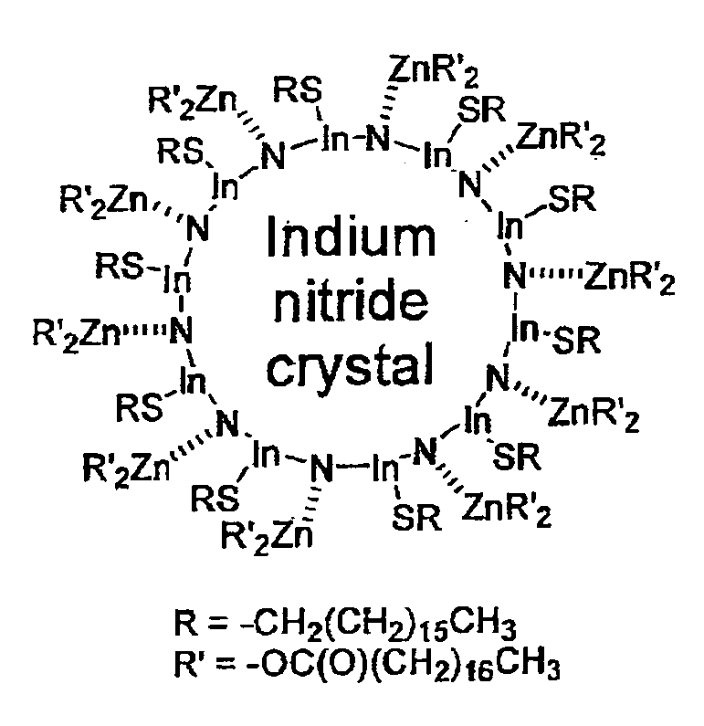
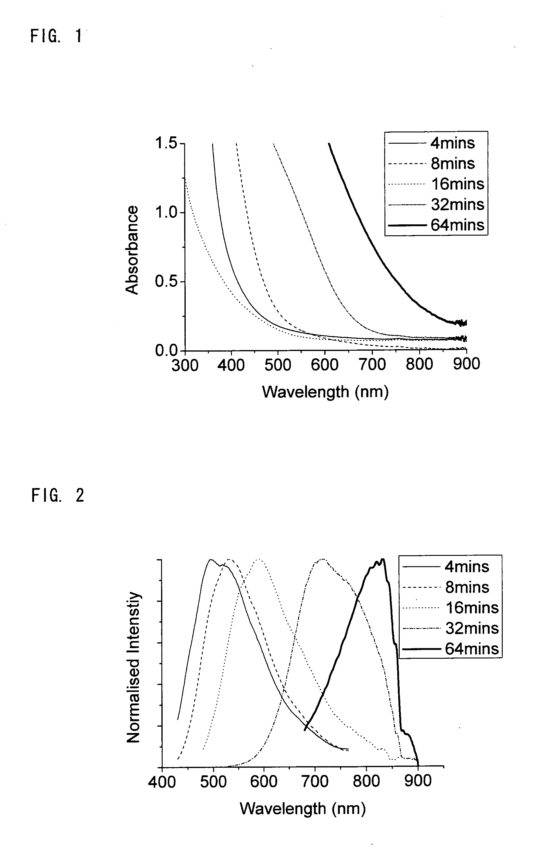
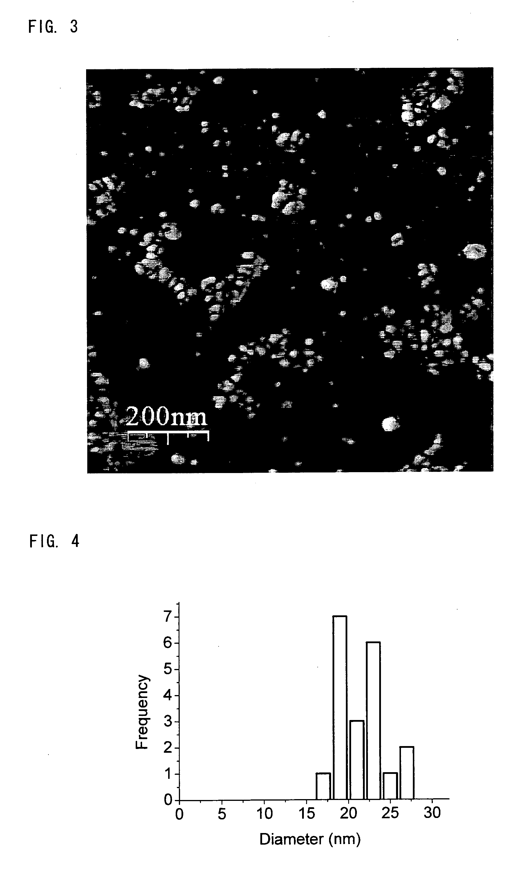
[0105]Indium iodide (300 mg, 0.6 mmol), sodium amide (500 mg, 12.8 mmol), hexadecane thiol (308 μl, 1.0 mmol), zinc stearate (379 mg, 0.6 mmol) and diphenyl ether (20 ml) were heated rapidly to 225° C. Of the constituents, Indium iodide provided a Group III metal (Indium), sodium amide provided nitrogen, hexadecane thiol is a capping agent with an electron-donating group, zinc stearate is a capping agent with an electron-accepting group and diphenyl ether acts as a solvent. Over the course of 60 minutes a number of 0.25 ml portions of the reaction mixture were removed and diluted with cyclohexane (3 ml) and any insoluble materials were removed using a centrifuge. The resulting clear solutions were analysed by absorption and emission spectroscopy and showed a change in the maximum emission wavelength from 480-850 nm over the course of the reaction, as shown in FIGS. 1 and 2. The peak in the emission spectrum has a full width at half the maximum intensity of the order of 150 nm.
[0106]...
example 2
[0113]Indium iodide (300 mg, 0.6 mmol), sodium amide (500 mg, 12.8 mmol), hexadecane thiol (308 μl, 1.0 mmol), zinc stearate (379 mg, 0.6 mmol) and diphenyl ether (20 ml) were heated rapidly to 250° C. Over the course of 40 minutes 0.25 ml portions of the reaction mixture were removed and diluted with cyclohexane (3 ml) and any insoluble material was removed using a centrifuge. This gives clear solutions of emissive indium nitride nanocrystals. As in example 1, the absorption / emission properties of the obtained nanoparticles depend on the reaction, and show a similar dependence on time to FIGS. 1 and 2.
example 3
[0114]Indium iodide (300 mg, 0.6 mmol), sodium amide (500 mg, 12.8 mmol), palmitic acid (256.4, 1.0 mmol), zinc stearate (379 mg, 0.6 mmol) and diphenyl ether (20 ml) were heated rapidly to 225° C. In this example, palmitic acid is used as a capping agent with an electron-donating group rather than hexadecane thiol.
[0115]Over the course of 40 minutes 0.25 ml portions of the reaction mixture were removed and diluted with cyclohexane (3 ml) and any insoluble material was removed using a centrifuge. This gives clear solutions of indium nitride nanocrystals. As in example 1, the absorption / emission properties of the obtained nanoparticles depend on the reaction, and show a similar dependence on time to FIGS. 1 and 2.
PUM
 Abstract
Description
Claims
Application Information